Display panel, manufacturing method thereof, and display device

A technology for display panels and display substrates, which is applied in the manufacturing of semiconductor/solid-state devices, semiconductor devices, electrical components, etc., can solve the problems of uneven film formation and complex thin-film packaging processes, avoid window effects, reduce production costs, and reduce The effect of complexity

Active Publication Date: 2020-04-03
SHANGHAI TIANMA MICRO ELECTRONICS CO LTD
View PDF4 Cites 0 Cited by
  • Summary
  • Abstract
  • Description
  • Claims
  • Application Information

AI Technical Summary

Problems solved by technology

[0005] Embodiments of the present invention provide a display panel, a manufacturing method thereof, and a display device, so as to solve the problems of complicated and uneven film formation in the existing thin film packaging process

Method used


Image

  • Display panel, manufacturing method thereof, and display device
  • Display panel, manufacturing method thereof, and display device
  • Display panel, manufacturing method thereof, and display device

Examples


Embodiment Construction

[0032] In order to make the purpose, technical solutions and advantages of the present invention clearer, the technical solutions of the present invention will be clearly and completely described through implementation with reference to the accompanying drawings in the embodiments of the present invention. Obviously, the described embodiments are the embodiment of the present invention. Some, but not all, embodiments. Based on the embodiments of the present invention, all other embodiments obtained by persons of ordinary skill in the art without making creative efforts belong to the protection scope of the present invention.

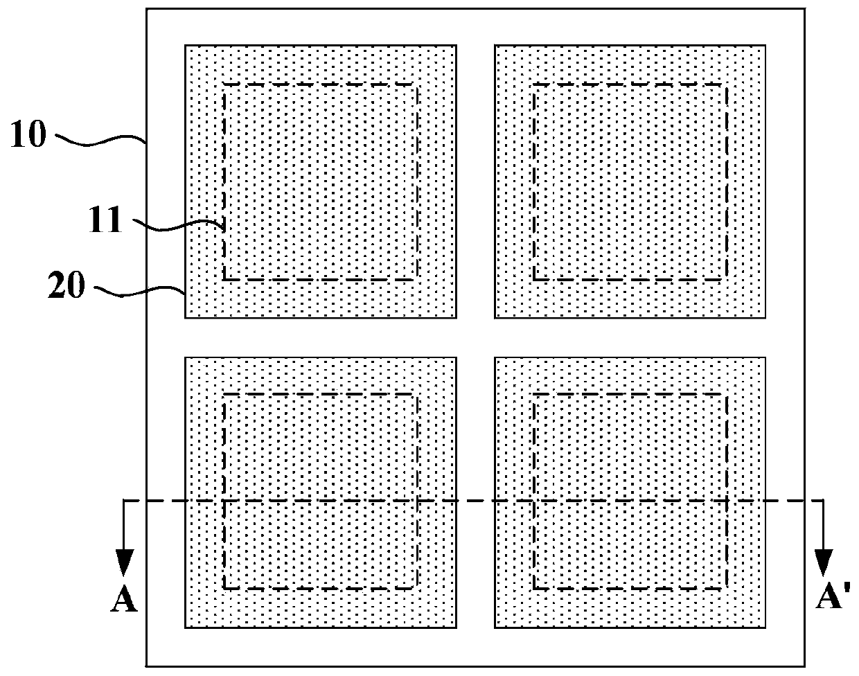
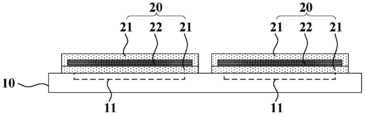
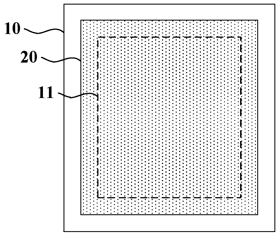
[0033] refer to figure 1 As shown in , it is a schematic diagram of a display panel provided by an embodiment of the present invention. The display panel provided in this embodiment includes: a display substrate 10, the display substrate 10 includes at least one display area 11; an encapsulation structure 20 encapsulating the display area 11, the encaps...


PUM

PropertyMeasurementUnit
thicknessaaaaaaaaaa
thicknessaaaaaaaaaa

Abstract

The embodiment of the present invention discloses a display panel, a manufacturing method thereof, and a display device. The display panel includes: a display substrate, the display substrate includes at least one display area; an encapsulation structure for encapsulating the display area, the encapsulation structure includes at least one inorganic layer and at least one organic layer, and the encapsulation structure is formed by first depositing each film layer and then etching. In the embodiment of the present invention, the packaging structure is formed by first depositing each film layer and then performing photolithography, so there is no need to use a mask to deposit the inorganic layer of the packaging structure, and it is not necessary to use a mask alignment system to align the mask. It reduces the complexity of the packaging process and the manufacturing cost; the thickness of the film layer of the packaging structure is uniform and the surface is flat, there will be no problem of uneven thickness in different regions caused by mask deposition, and the window effect of mask deposition is avoided.

Description

technical field [0001] Embodiments of the present invention relate to display technologies, and in particular to a display panel, a manufacturing method thereof, and a display device. Background technique [0002] With the development of display technology, the application of flexible display technology is becoming more and more extensive. The existing flexible organic light emitting display panel structure generally includes a flexible substrate, a display device layer, and a thin film encapsulation layer. The thin film encapsulation layer generally includes an inorganic layer and an organic layer, the inorganic layer is used to block water and oxygen, and the organic layer is used to improve the flexibility of the thin film encapsulation layer. [0003] In a flexible organic light-emitting display panel, the inorganic layer of the thin film encapsulation layer is usually deposited after alignment using a mask mask. Specifically, before forming the thin film encapsulation...

Claims


Application Information

Patent Timeline
Patent Type & Authority Patents(China)
IPC IPC(8): H01L51/52H01L51/56
CPCH10K50/8445H10K71/00
Inventor 冷传利李针英
Owner SHANGHAI TIANMA MICRO ELECTRONICS CO LTD
Why Eureka
Try Eureka