Active region structure and method of forming same
一种有源区域、有源层的技术,应用在半导体器件、电气元件、晶体管等方向,能够解决损毁、存储单元操作不稳定等问题,达到避免损坏的效果
- Summary
- Abstract
- Description
- Claims
- Application Information
AI Technical Summary
Problems solved by technology
Method used
Image
Examples
Embodiment Construction
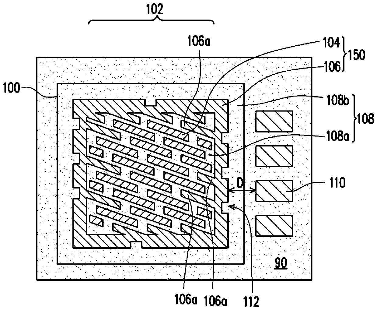
[0050] Semiconductor elements, such as memory cells, need to be isolated to achieve the effect of insulation, and the insulating structure is formed between these element units and between these elements under the requirement of high element density, for example, by means of a shallow trench insulation layer. Between the unit and the surrounding active area to provide insulation between components.
[0051] The invention considers the insulation quality between components and proposes a corresponding design.
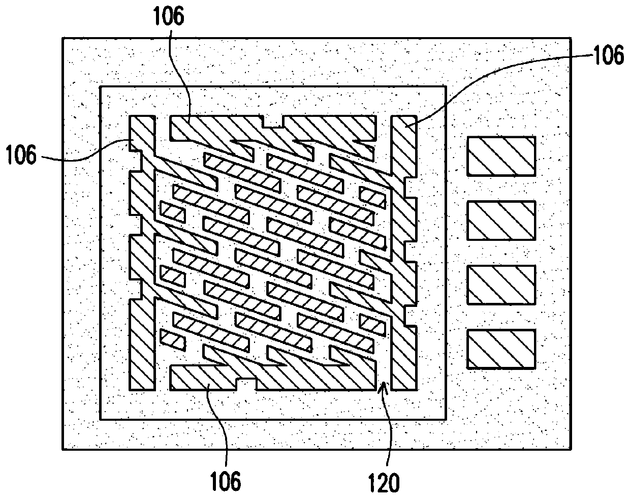
[0052] The material of the shallow trench insulation layer is a dielectric material, and the element unit and the peripheral active area are formed by a part of the substrate, such as the surface layer of the silicon substrate, which is formed after patterning. Furthermore, the distance between the element units and the peripheral active area is larger than the gap between these element units, and occupying a larger area produces greater stress. Therefore, the material ...
PUM
 Abstract
Description
Claims
Application Information
 - R&D Engineer
- R&D Manager
- IP Professional
- Industry Leading Data Capabilities
- Powerful AI technology
- Patent DNA Extraction
Browse by: Latest US Patents, China's latest patents, Technical Efficacy Thesaurus, Application Domain, Technology Topic, Popular Technical Reports.
© 2024 PatSnap. All rights reserved.Legal|Privacy policy|Modern Slavery Act Transparency Statement|Sitemap|About US| Contact US: help@patsnap.com


