
Large-scale processing integration method for atomic devices

An integrated method and large-scale technology, applied in the field of microelectronics technology, can solve the problems of inability to meet the processing and integration requirements of a large number of atomic devices, and the low efficiency of single-atom manipulation, so as to achieve efficient processing and integration, and meet a large number of easy-to-implement requirements. Effect

Inactive Publication Date: 2018-03-20
苏州康力丰纳米科技有限公司
View PDF6 Cites 0 Cited by
  • Summary
  • Abstract
  • Description
  • Claims
  • Application Information

AI Technical Summary

Problems solved by technology

However, the efficiency of single-atom manipulation is too low to meet the demands of mass-atom device processing and integration.

Method used


Image

  • Large-scale processing integration method for atomic devices
  • Large-scale processing integration method for atomic devices

Examples


Embodiment 1

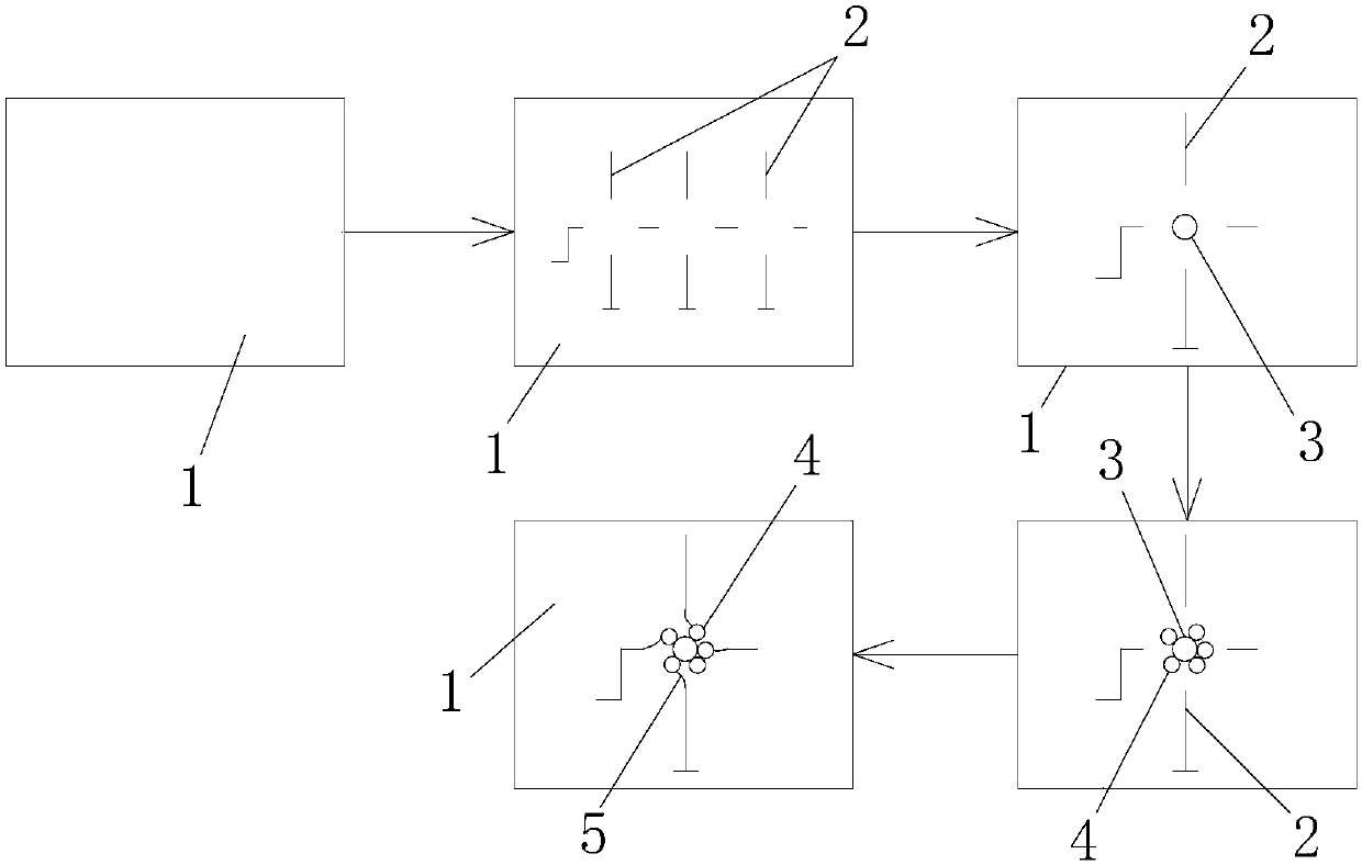
[0034] Embodiment 1, with reference to figure 1 , the large-scale processing and integration method of atomic-level devices is based on a typical processing and operation scheme combining top-down and bottom-up, the specific process is as follows,

[0035] 1) Process a batch of peripheral circuits 2 on the substrate of the substrate 1 by using photolithography and electron beam lithography;

[0036] 2) Use the method of light field manipulation to control the distribution of the potential field in space, and settle a seed 3 in the designated micro-area;

[0037] 3), according to the selectivity of atoms and molecules, grow the device core 4 around the seed 3;

[0038] 4) According to the selectivity of atomic molecules, the device core 4 adsorbs the black atomic chain 5 to realize the connection with the peripheral circuit 2 to form a large-scale atomic-level device.

Embodiment 2

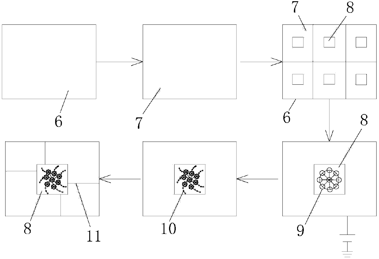
[0039] Embodiment 2, with reference to figure 2 , the method for large-scale processing and integration of atomic-level devices, a large-scale cluster device processing scheme based on electrical guidance, the specific process is as follows,

[0040] 1), plating a layer of silver (Ag) film 7 on the substrate of the substrate 6;

[0041] 2), using photolithography and electron beam lithography to process a window 8 of 10×10 nanometers on the silver film 7;

[0042] 3), the Au 13 The (gold) cluster 9 is accelerated to 100 electron volts and deposited on the substrate 6, and a voltage of 100-105V is applied to the silver film 7 of the substrate 6 to ensure that the atomic cluster reaches the window 8;

[0043] 4), through Au 13 The selective adsorption of clusters 9 and thiols makes the entire substrate 6 lightly covered with a layer of thiols 10, and then washed away, under selective and molecular-level guidance, to form Au 13 The cluster 9 is connected to the thiol layer 1...


PUM


Abstract

The invention discloses a large-scale processing integration method for atomic devices. Through the from-top-to-bottom microelectronics technology and the from-bottom-to-up microelectronics technology, efficient processing and integration of the atomic devices are achieved. Through the from-top-to-bottom technology including photoetching and electron beam lithography, an external connecting electrode with the nanoscale and the larger size is manufactured. Through the from-bottom-to-up technology including a scanning tunneling microscope, cluster equipment and the like applying, atomic materials grow at target positions and are successfully connected with the external connecting electrode. Under the background that the Moore's law is about to failure, the atomic devices and a circuit manufacturing path are easy to achieve, the efficiency is high, and the processing and integration requirements of a large number of atomic devices are met.

Description

technical field [0001] The invention relates to the technical field of microelectronic technology, in particular to a processing method for an atomic-level device. Background technique [0002] From the 1970s to the present, Moore's Law has dominated the microelectronics industry, and the feature size from microns has gradually reached 5 nanometers. In this process, with the reduction of feature size, the operation speed of devices is getting faster and faster, resulting in the most significant technological progress and happiness experience in human society. The key factor is the photolithography micromachining process. In this process, people use a mask to selectively block the light path to achieve patterning on metal and silicon substrates. With this as the core, this top-down process route is the cornerstone of today's microelectronics process. [0003] However, in 2016, the international authoritative academic journal "Nature" announced that Moore's Law has expired....

Claims


Application Information

Patent Timeline
Patent Type & Authority Applications(China)
IPC IPC(8): B82B1/00B82B3/00B82Y40/00
CPCB82B1/001B82B3/0019B82Y40/00
Inventor 王学锋宋凤麒
Owner 苏州康力丰纳米科技有限公司
Learn More