High electron mobility transistor and manufacturing method thereof

A technology with high electron mobility and manufacturing method, applied in the direction of semiconductor/solid-state device manufacturing, circuits, electrical components, etc., can solve the problems of large etching damage, dangerous operation, poor process compatibility, etc., achieve large on-current, reduce Interface state, the effect of avoiding damage

Inactive Publication Date: 2018-03-06
PEKING UNIV SHENZHEN GRADUATE SCHOOL
View PDF7 Cites 5 Cited by
  • Summary
  • Abstract
  • Description
  • Claims
  • Application Information

AI Technical Summary

Problems solved by technology

As for the etching method of the gate area, it is divided into two methods: dry method and wet method. The reliability cannot be guaranteed, and it is not suitable for the development of mass production processes; the wet etching solution is an effective means to solve the problem of dry etching damage, but it also has its own disadvantages, such as poor process compatibility, pollution of existing process platforms, and complex processes. operational hazards, etc.

Method used


Image

  • High electron mobility transistor and manufacturing method thereof
  • High electron mobility transistor and manufacturing method thereof
  • High electron mobility transistor and manufacturing method thereof

Examples


Embodiment Construction

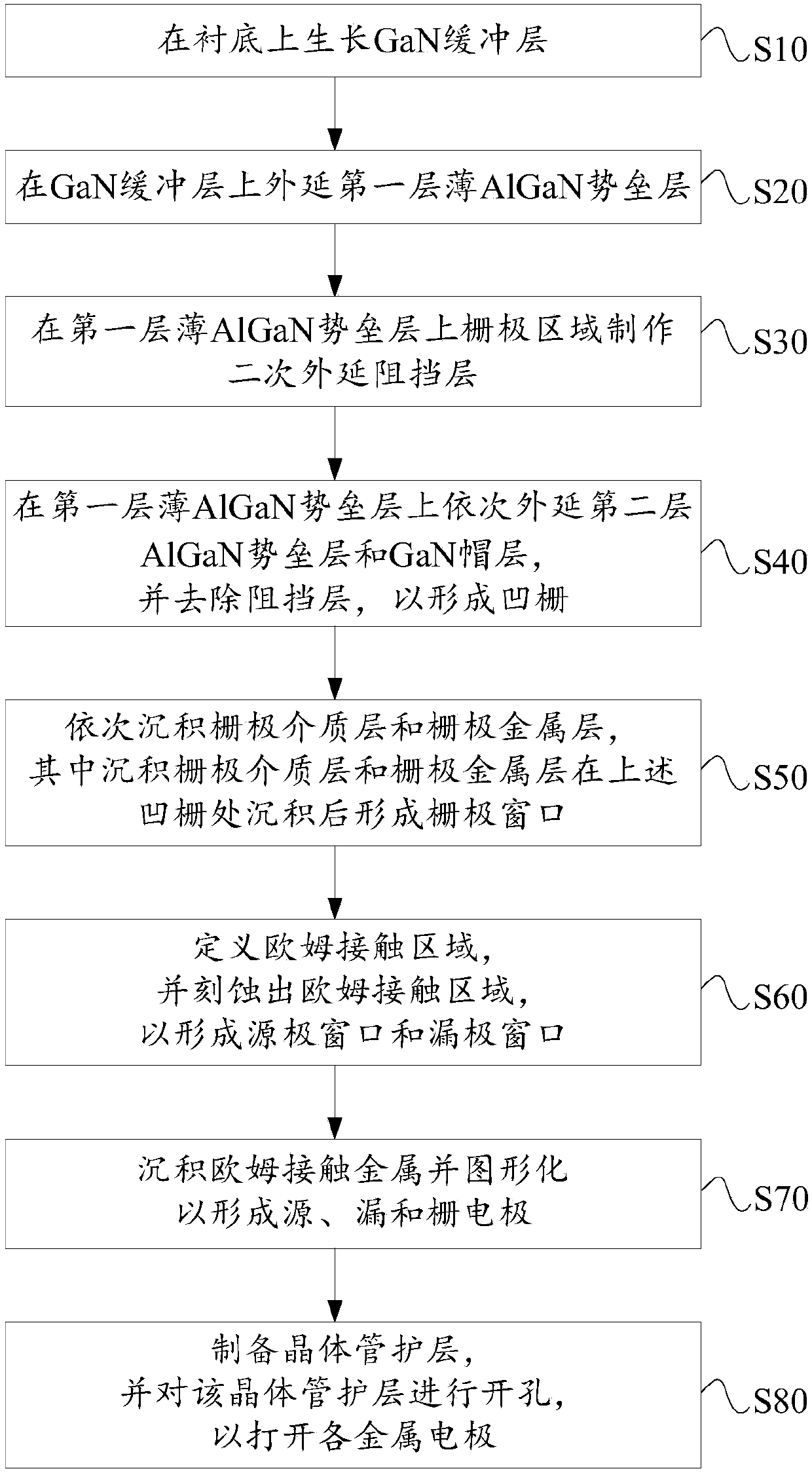
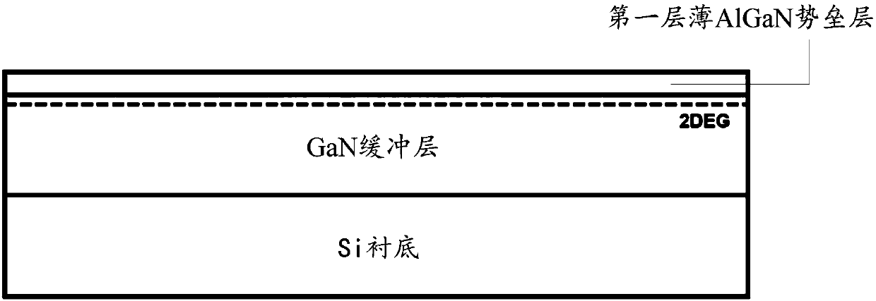
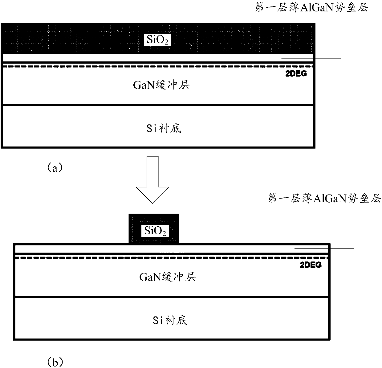
[0033] The present invention will be further described in detail below through specific embodiments in conjunction with the accompanying drawings. Wherein, similar elements in different implementations adopt associated similar element numbers. In the following implementation manners, many details are described for better understanding of the present application. However, those skilled in the art can readily recognize that some of the features can be omitted in different situations, or can be replaced by other elements, materials, and methods. In some cases, some operations related to the application are not shown or described in the description, this is to avoid the core part of the application being overwhelmed by too many descriptions, and for those skilled in the art, it is necessary to describe these operations in detail Relevant operations are not necessary, and they can fully understand the relevant operations according to the description in the specification and genera...


PUM

PropertyMeasurementUnit
Thicknessaaaaaaaaaa

Abstract

The invention discloses a high electron mobility transistor and a manufacturing method thereof. A recessed gate is formed through manufacturing a secondary epitaxial barrier layer in a gate area on afirst thin AlGaN barrier layer, epitaxially growing a second AlGaN barrier layer and a GaN cap layer on the first thin AlGaN barrier layer in sequence and removing the barrier layer. Therefore, any dry and wet etching process is not needed when the recessed gate is manufactured, the damage of etching to the surfaces of the AlGaN barrier layers is avoided and the interface state is reduced to ensure excellent performance of the transistor; and in addition, the recessed gate is achieved through secondary epitaxy of AlGaN, so that the transistor has double AlGaN barrier layers, sufficient electrons in a channel are ensured and the transistor has relatively high breakover current.

Description

technical field [0001] The invention relates to the field of semiconductors, in particular to a high electron mobility transistor and a manufacturing method thereof. Background technique [0002] Gallium nitride (GaN) material has a large band gap, high critical breakdown field strength, fast electron saturation and drift speed, and can form a high-concentration two-dimensional electron gas and channel electrons without doping with the heterojunction of AlGaN material. The high mobility and other properties make it the material of choice for the preparation of high-frequency and high-power microwave transistors. [0003] In 1979, T.Mimura proposed the concept of High Electron Mobility Transistor (HEMT) for the first time, and produced a depletion-type AlGaAs / GaAs HEMT device in the second year, and an enhancement-type device also appeared in the same year . Research on AlGaN / GaN HEMTs began in 1992. In 1992, Khan et al. from APA Optical Company of the United States success...

Claims


Application Information

Patent Timeline
IPC IPC(8): H01L21/335H01L21/28H01L29/778H01L29/423
CPCH01L29/401H01L29/42316H01L29/66462H01L29/7783
Inventor 孙辉刘美华林信南陈东敏
Owner PEKING UNIV SHENZHEN GRADUATE SCHOOL
Why Eureka
Try Eureka