Method and structure for forming a double-gate fin field effect transistor

A field-effect transistor and double-gate technology, which is applied in the field of formation method and structure of double-gate fin field-effect transistors, can solve problems such as the difference between the upper and lower parts of the fin, and high leakage, so as to reduce leakage, improve device performance, and change threshold voltage Effect

Active Publication Date: 2020-12-25
SHANGHAI HUALI MICROELECTRONICS CORP
View PDF1 Cites 0 Cited by
  • Summary
  • Abstract
  • Description
  • Claims
  • Application Information

AI Technical Summary

Problems solved by technology

[0004] However, in mass production, on the one hand, because the ion implantation process is difficult to distribute evenly in the vertical direction of the fin, there are differences between the upper and lower parts of the fin
On the other hand, the effective channel bottom leakage of fin is higher

Method used


Image

  • Method and structure for forming a double-gate fin field effect transistor
  • Method and structure for forming a double-gate fin field effect transistor
  • Method and structure for forming a double-gate fin field effect transistor

Examples


Embodiment Construction

[0053] The invention provides a double-gate fin field effect transistor and a forming method thereof.

[0054] In the following, the present invention will be described in detail and specifically through specific examples, so as to better understand the present invention, but the following examples do not limit the scope of the present invention.

[0055] Such as Figure 9 As shown in the flow chart of the present invention, a method for forming a double-gate fin field effect transistor in a preferred embodiment of the present invention includes the following steps:

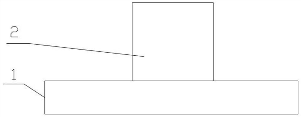
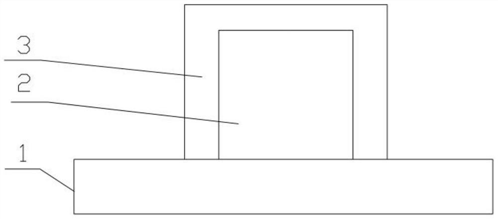
[0056] Such as figure 2 As shown, S1 provides a semiconductor substrate (not shown), on which a buried oxide layer 1 is formed;

[0057] S2 forming a first semiconductor layer (not shown) on the buried oxide layer 1, and patterning the first semiconductor layer to form a semiconductor fin layer 2;

[0058] The method for forming the semiconductor fin layer 2 is to first deposit a first semiconductor layer on ...


PUM

PropertyMeasurementUnit
thicknessaaaaaaaaaa

Abstract

The invention discloses a method for effectively optimizing a fin type field-effect transistor structure, a fin type field-effect transistor prepared through the method and a formation method of the fn type field-effect transistor, wherein a plurality of gate dielectric layers are arranged in the vertical direction of a fin, and electric leakage on the bottom of an effective channel of the fin iseffectively reduced. According to the provided bigrid fin type field-effect transistor structure, a grid electrode is formed on the outer side face of the fin to serve as a control grid, another gridelectrode is formed on the inner side face of the fin to serve as a drive grid, the structure not only can reduce electric leakage on the bottom of the effective channel of the fin, by regulating thethickness of the control grid, the threshold voltage of the drive grid can be effectively changed, and the performance of the device also can be improved.

Description

technical field [0001] The invention relates to a semiconductor preparation process, in particular to a method and structure for forming a double gate fin field effect transistor. Background technique [0002] As the size of semiconductor devices becomes smaller and smaller, the short channel effect becomes more and more obvious. In order to suppress the short channel effect, a FinFET (Fin Field-Effect Transistor) formed on a silicon-on-insulator (SOI, Silicon-On-Insulator) wafer or a bulk semiconductor substrate is proposed. A FinFET includes a channel region formed in the middle of a fin (fin) of semiconductor material, and source / drain regions formed at both ends of the fin. The gate electrode surrounds the channel region on both sides of the channel region (ie a double gate structure), thereby forming an inversion layer on each side of the channel. Since the entire channel region can be controlled by the gate, it can play a role in suppressing the short channel effect....

Claims


Application Information

Patent Timeline
Patent Type & Authority Patents(China)
IPC IPC(8): H01L29/78H01L21/8234
CPCH01L21/823431H01L21/82345H01L29/785H01L2924/13085
Inventor 鲍宇
Owner SHANGHAI HUALI MICROELECTRONICS CORP
Why Eureka
Try Eureka