


Quick Research
Generate reliable direction feasibility study reports for your R&D in just a few steps.

Technical Q&A
Discover and master advanced knowledge NOW. Basics, ideas, possibilities, all at once.

Find Solutions
As an expert in R&D theories, this can generate solutions to your technical problems instantly.

Evaluate Feasibility
Analyze your overall solution with one click, know your potential R&D risks in advance.

Monitor Landscape
Get weekly tech updates, stay abreast of the latest tech innovations and key insights.
Semiconductor device structure and fabrication method thereof
A device structure and semiconductor technology, applied in the fields of semiconductor devices, semiconductor/solid-state device manufacturing, electrical components, etc., can solve the problems of low yield of critical size chips, etc.
- Summary
- Abstract
- Description
- Claims
- Application Information
AI Technical Summary
Problems solved by technology
Method used
Image

Examples
Embodiment 1
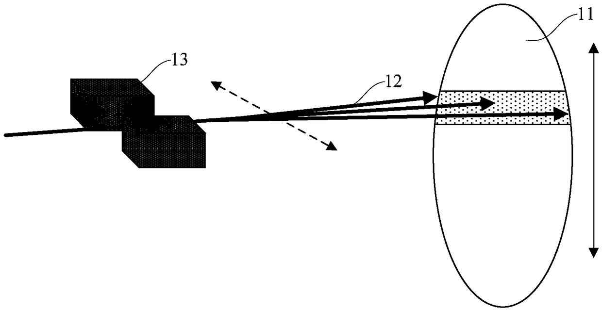
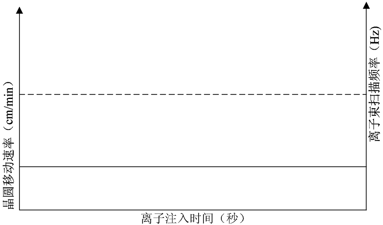
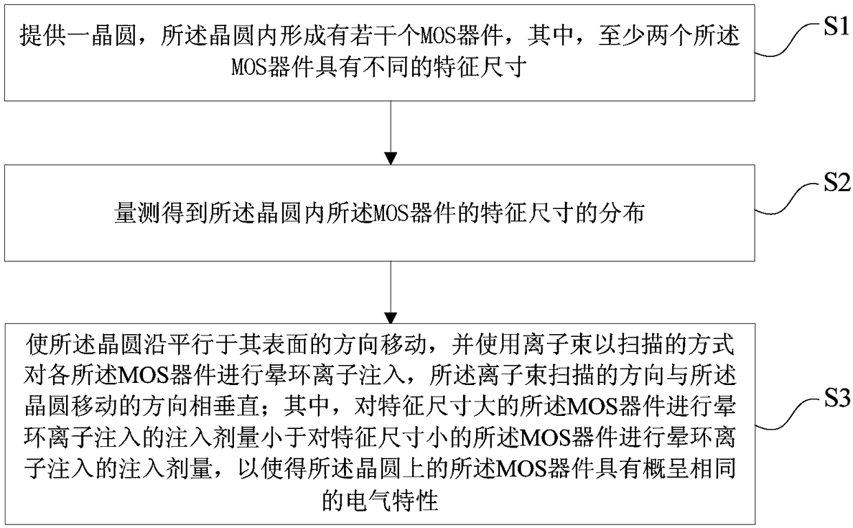
[0062] see figure 1 , the invention provides a kind of preparation method of semiconductor device structure, the preparation method of described semiconductor device structure comprises the following steps:
[0063] 1) providing a wafer in which several MOS devices are formed, wherein at least two of the MOS devices have different feature sizes;
[0064] 2) measuring and obtaining the distribution of the characteristic sizes of the MOS devices in the wafer;
[0065] 3) moving the wafer in a direction parallel to its surface, and performing halo ion implantation on each of the MOS devices in a scanning manner using an ion beam, the scanning direction of the ion beam is the same as the moving direction of the wafer The directions are perpendicular; wherein, the implantation dose of halo ion implantation for the MOS device with a large feature size is smaller than the implantation dose for halo ion implantation for the MOS device with a small feature size, so that the The MOS d...
Embodiment 2
[0091] Please continue to refer to Embodiment 1 Figure 4 to Figure 15 , the present invention also provides a semiconductor device structure, the semiconductor device structure is prepared by the preparation method described in Embodiment 1, the semiconductor device structure includes: a number of MOS devices arranged at intervals, wherein at least two Each of the MOS devices has different feature sizes; an annular halo implantation region 25 is formed in the channel of each of the MOS devices, and the ion implantation concentration in the halo implantation region 25 is inversely proportional to that of the MOS device. Feature size.
[0092] As an example, the ion implantation concentration in the halo implantation region 25 in the MOS device with a relatively large feature size is lower than the ion implantation concentration in the halo implantation region 25 in the MOS device with a small relative feature size, , to ensure that the MOS devices on the wafer 21 have substan...
PUM
 Abstract
Description
Claims
Application Information
 - R&D Engineer
- R&D Manager
- IP Professional
- Industry Leading Data Capabilities
- Powerful AI technology
- Patent DNA Extraction
Browse by: Latest US Patents, China's latest patents, Technical Efficacy Thesaurus, Application Domain, Technology Topic, Popular Technical Reports.
© 2024 PatSnap. All rights reserved.Legal|Privacy policy|Modern Slavery Act Transparency Statement|Sitemap|About US| Contact US: help@patsnap.com