Method of growth morphology and component control over plane germanium silicon and relative nanowires based on heterogeneous laminated amorphous film supply
A technology of amorphous thin film and nanowire, which is applied in the direction of nanotechnology, nanotechnology, nanostructure manufacturing, etc., can solve the problem of low compatibility of standard silicon processes, limitations of large-scale device integration of VLS nanowires, and functional applications, micro High operating costs and other issues
- Summary
- Abstract
- Description
- Claims
- Application Information
AI Technical Summary
Problems solved by technology
Method used
Image
Examples
Embodiment 1
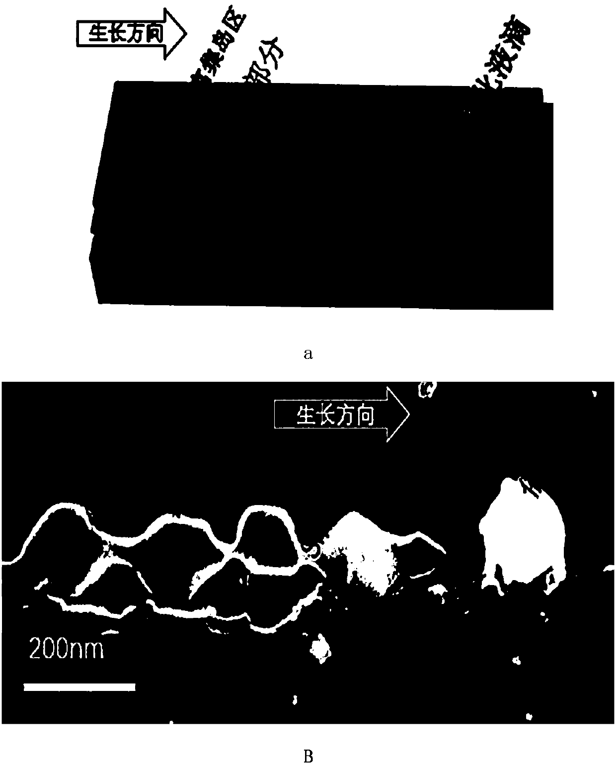
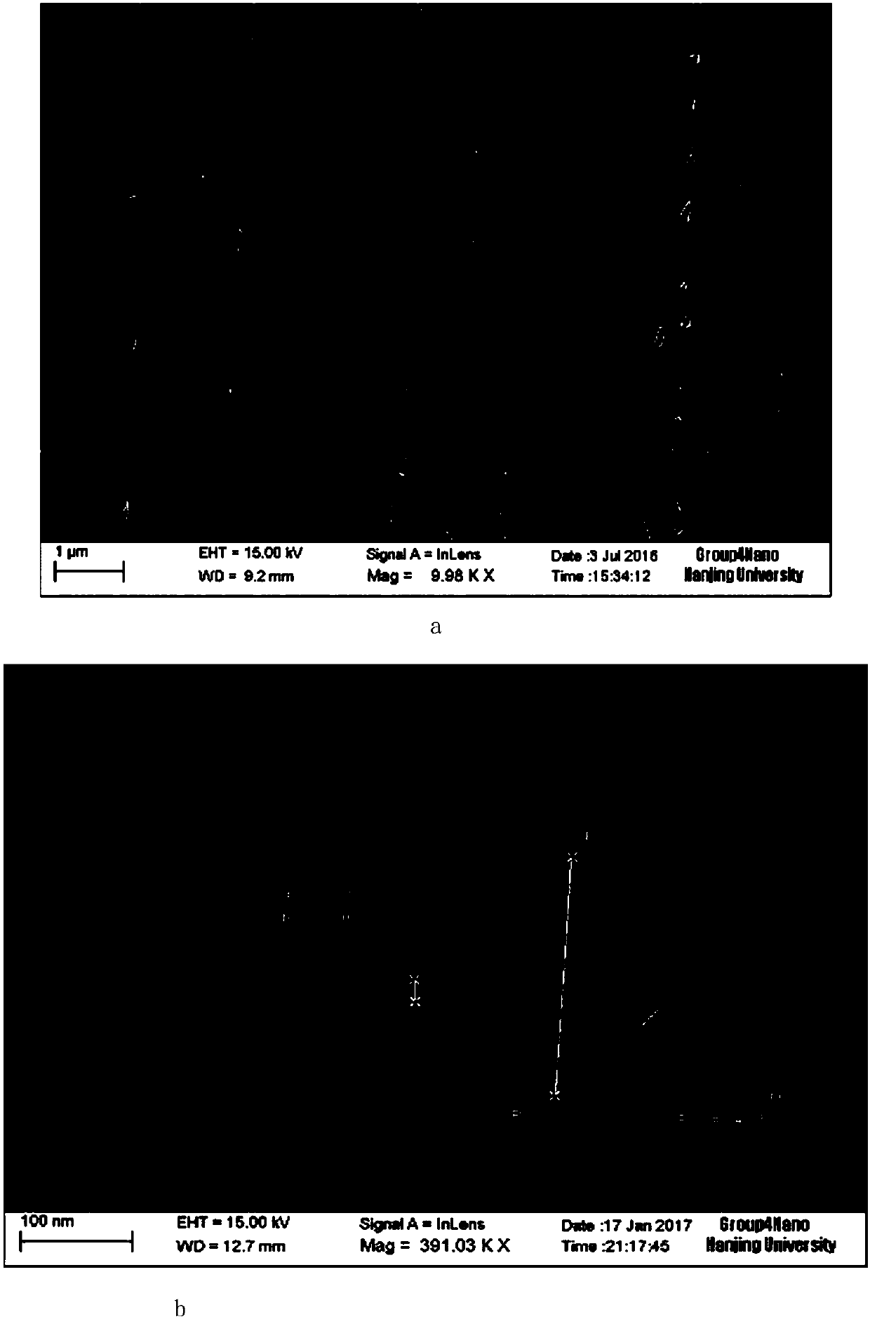
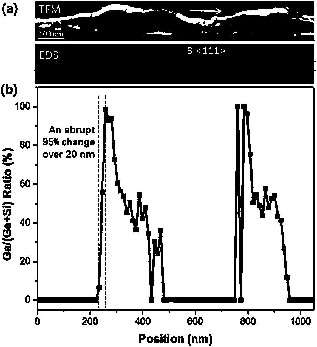
[0028] Example 1, In (indium)-induced growth of germanium-rich junction region ~ 160nm diameter ~ 40nm silicon germanium wire, Ge (germanium) content periodically changes the method for directional growth of germanium-enriched island-shaped planar silicon-germanium heterojunction nanowires .
[0029] A 500 μm silicon-based substrate with a silicon dioxide layer thickness of 300 nm was used to obtain a clean substrate through an RCA standard cleaning process.
[0030] 1) A photolithographic sample with a corresponding pattern was prepared using a photolithographic plate with a strip width of 3 μm and a spacing of 3 μm. After ICP etching to a depth of ~150 nm, it was cleaned with acetone, and the photoresist was washed away before secondary photolithography was performed. The second photolithography is perpendicular to the photolithographic pattern obtained by ICP etching, and a photolithographic sample with a strip width of 10 μm and a strip spacing of 100 μm is prepared. A 30...
Embodiment 2
[0034] Example 2, Sn (tin) induced growth of germanium-rich junction region ~ 160nm diameter ~ 40nm silicon germanium wire, Ge (germanium) content periodically changes the method for directional growth of germanium-enriched island-shaped planar silicon-germanium heterojunction nanowires .
[0035] A 500 μm silicon-based substrate with a silicon dioxide layer thickness of 300 nm was used to obtain a clean substrate through an RCA standard cleaning process.
[0036] 1) A photolithographic sample with a corresponding pattern was prepared using a photolithographic plate with a strip width of 3 μm and a spacing of 3 μm. After ICP etching to a depth of ~150 nm, it was cleaned with acetone, and the photoresist was washed away before secondary photolithography was performed. The second photolithography is perpendicular to the photolithographic pattern obtained by ICP etching, and a photolithographic sample with a strip width of 10 μm and a strip spacing of 100 μm is prepared. A 30 nm...
Embodiment 3
[0040] Example 3, In, Sn (indium, tin alloy) induced growth germanium-rich junction region ~ 160nm diameter ~ 40nm silicon germanium line, Ge (germanium) content periodically changes direction growth germanium-enriched island-shaped planar silicon-germanium heterogeneity Methods for knotting nanowires.
[0041] A 500 μm silicon-based substrate with a silicon dioxide layer thickness of 300 nm was used to obtain a clean substrate through an RCA standard cleaning process.
[0042] 1) A photolithographic sample with a corresponding pattern was prepared using a photolithographic plate with a strip width of 3 μm and a spacing of 3 μm. After ICP etching to a depth of ~150 nm, it was cleaned with acetone, and the photoresist was washed away before secondary photolithography was performed. The second photolithography is perpendicular to the photolithographic pattern obtained by ICP etching, and a photolithographic sample with a strip width of 10 μm and a strip spacing of 100 μm is prep...
PUM
 Abstract
Description
Claims
Application Information
 - Generate Ideas
- Intellectual Property
- Life Sciences
- Materials
- Tech Scout
- Unparalleled Data Quality
- Higher Quality Content
- 60% Fewer Hallucinations
Browse by: Latest US Patents, China's latest patents, Technical Efficacy Thesaurus, Application Domain, Technology Topic, Popular Technical Reports.
© 2025 PatSnap. All rights reserved.Legal|Privacy policy|Modern Slavery Act Transparency Statement|Sitemap|About US| Contact US: help@patsnap.com


