
Patsnap Eureka
For R&D, Patsnap Eureka makes reading and utilizing patents & technical documents easy.
Patsnap Eureka AIR
Designed for self-driven R&D workflows. Generate viable solutions, solve complex R&D challenges, empower your innovation with AI.

Patsnap Eureka Materials
Designed for material experts only. Revolutionize your material R&D, from search, analyze, to developing new materials.

TechResearch
Generate reliable direction feasibility study reports for your R&D in just a few steps.

TechSeek
Discover and master advanced knowledge NOW. Basics, ideas, possibilities, all at once.

TechMind
As an expert in R&D Theories, TechMind can generates customized viable solutions instantly.

TechRisk
Analyze your overall solution with one click, know your potential R&D risks in advance.

TechMonitor
Get weekly tech updates, stay abreast of the latest tech innovations and key insights.
How to make a display panel
A manufacturing method and technology for display panels, which are applied in semiconductor/solid-state device manufacturing, electrical components, circuits, etc., can solve problems such as damage to circuits, waste of motherboard materials, and reduction in typesetting utilization.
- Summary
- Abstract
- Description
- Claims
- Application Information
AI Technical Summary
Problems solved by technology
Method used
Image

Examples
Embodiment Construction
[0034] The following examples are provided for detailed description, and the examples are only used as examples for illustration, and are not intended to limit the scope of protection of the present invention. The same / similar symbols are used to represent the same / similar components in the following description.
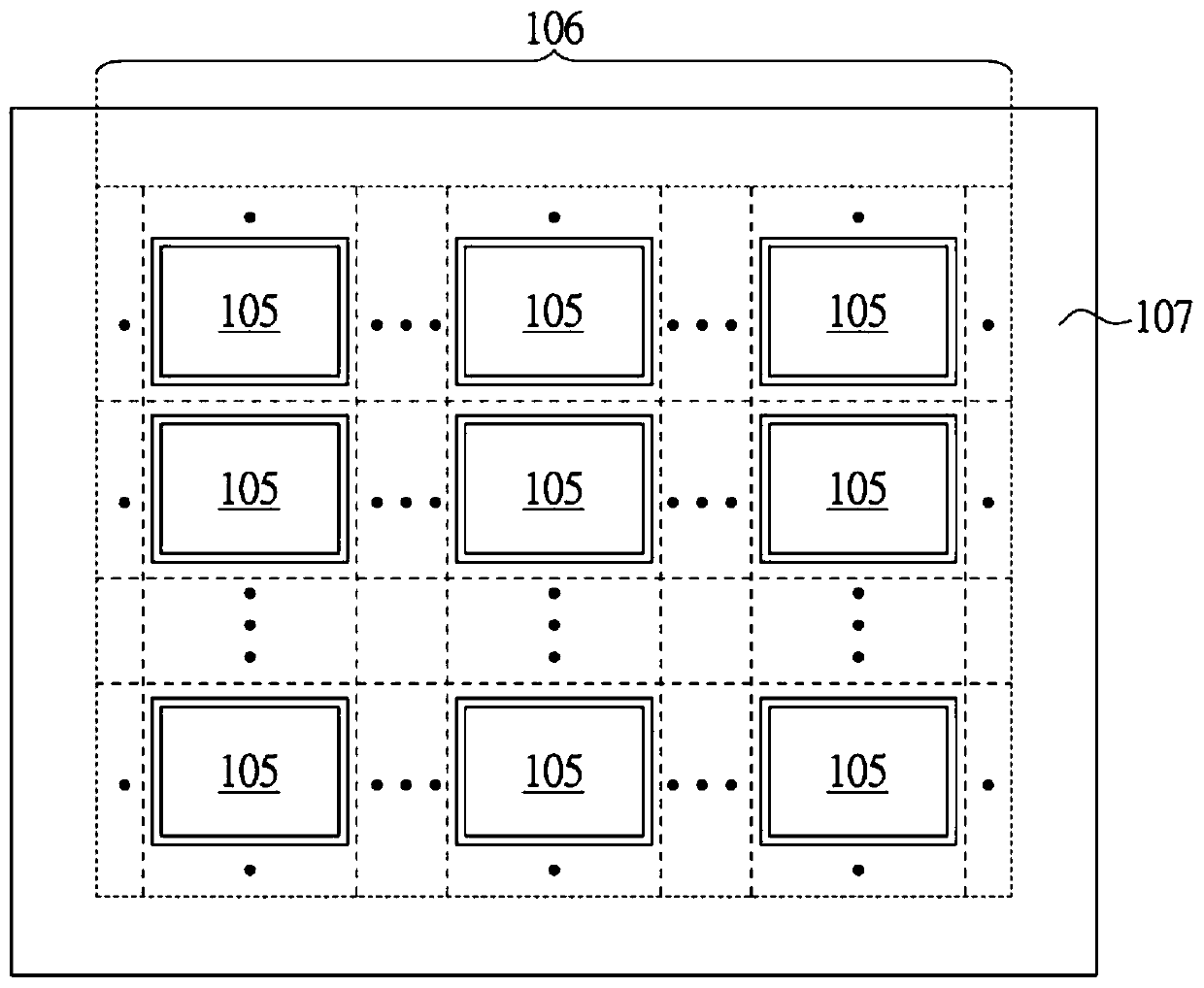
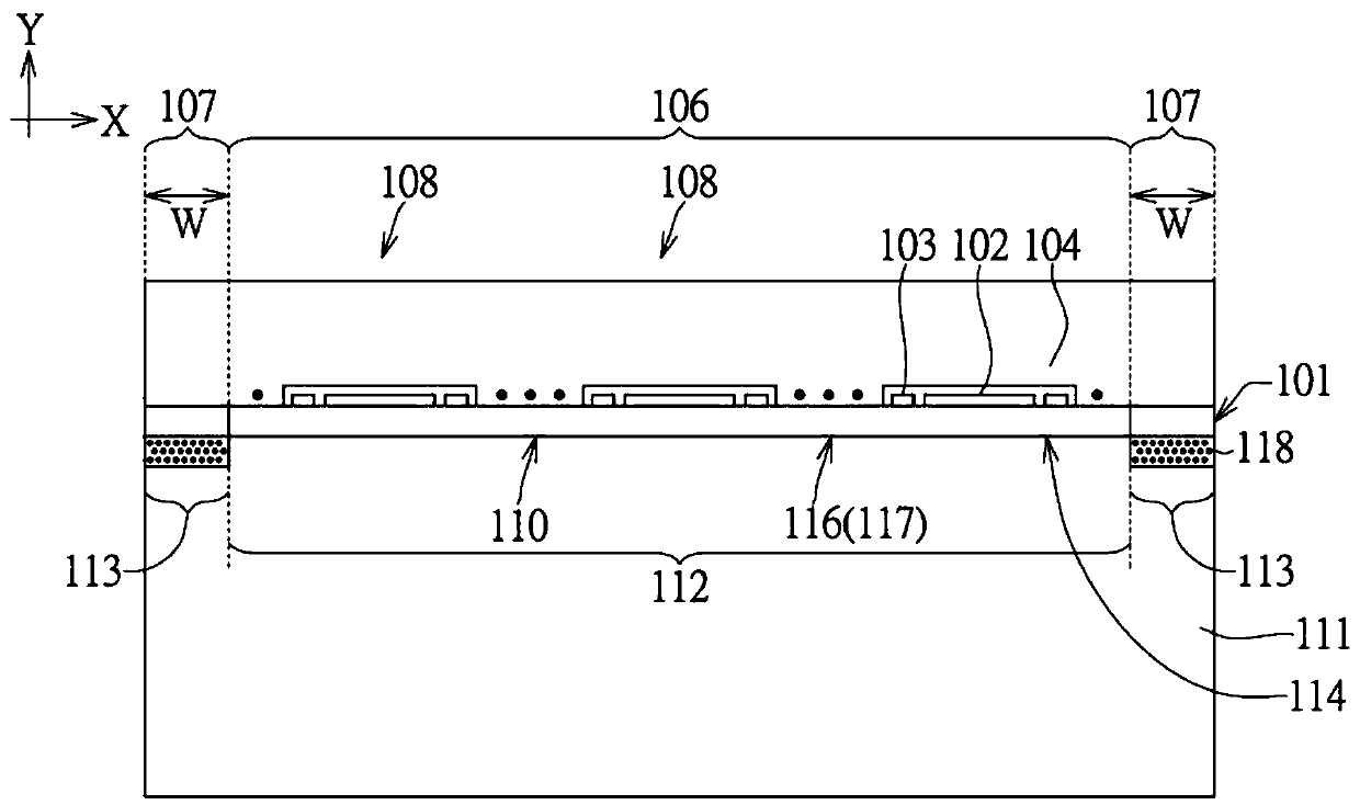
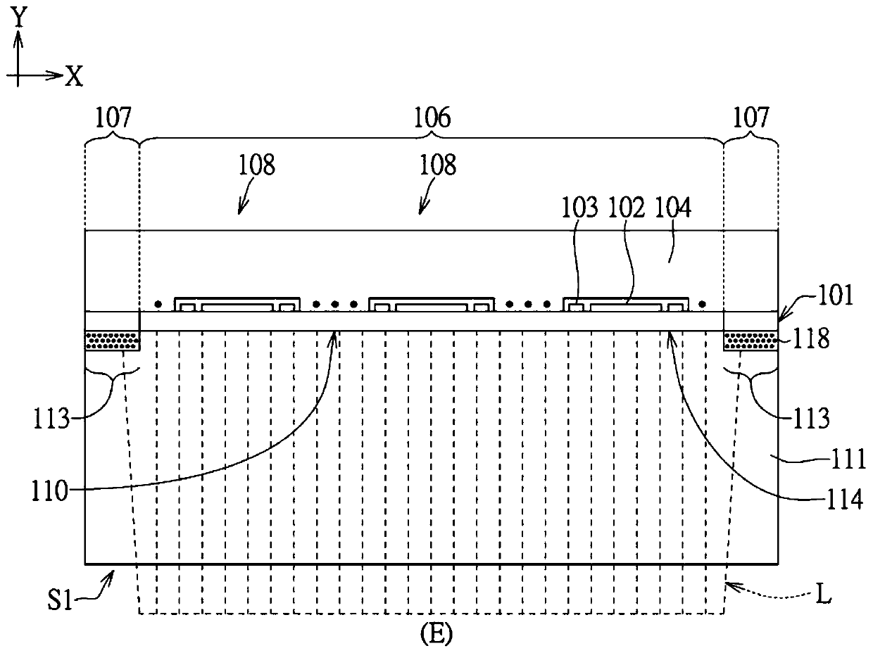
[0035] Please refer to Figure 1A to Figure 1C , the manufacturing method of the display panel 108 according to an embodiment of the present invention includes the following steps. First, please refer to Figure 1A and Figure 1B , forming a motherboard 101 on a carrier 111 , wherein the motherboard 101 is a substrate material for making the display panel 108 and can be used as a flexible substrate. In this embodiment, the motherboard 101 is temporarily formed on the supporting hard carrier 111, and in a subsequent stage, the pixel unit 102, the circuit layer 103 and the protective layer 104 required by the display panel 108 can be fabricated. After completion, t...
PUM
 Abstract
Description
Claims
Application Information
 - R&D Engineer
- R&D Manager
- IP Professional
- Industry Leading Data Capabilities
- Powerful AI technology
- Patent DNA Extraction
Browse by: Latest US Patents, China's latest patents, Technical Efficacy Thesaurus, Application Domain, Technology Topic, Popular Technical Reports.
© 2024 PatSnap. All rights reserved.Legal|Privacy policy|Modern Slavery Act Transparency Statement|Sitemap|About US| Contact US: help@patsnap.com