Zinc oxide ink and preparation method thereof, electron transmission membrane layer and display device
A technology of zinc oxide and zinc oxide nanometers, applied in chemical instruments and methods, inks, circuits, etc., can solve the problems of forming black spots, affecting the quality of the film layer, and the film layer is prone to a large number of holes, so as to avoid aggregation and increase space Steric hindrance, quality improvement effect
- Summary
- Abstract
- Description
- Claims
- Application Information
AI Technical Summary
Problems solved by technology
Method used
Image
Examples
Embodiment 1
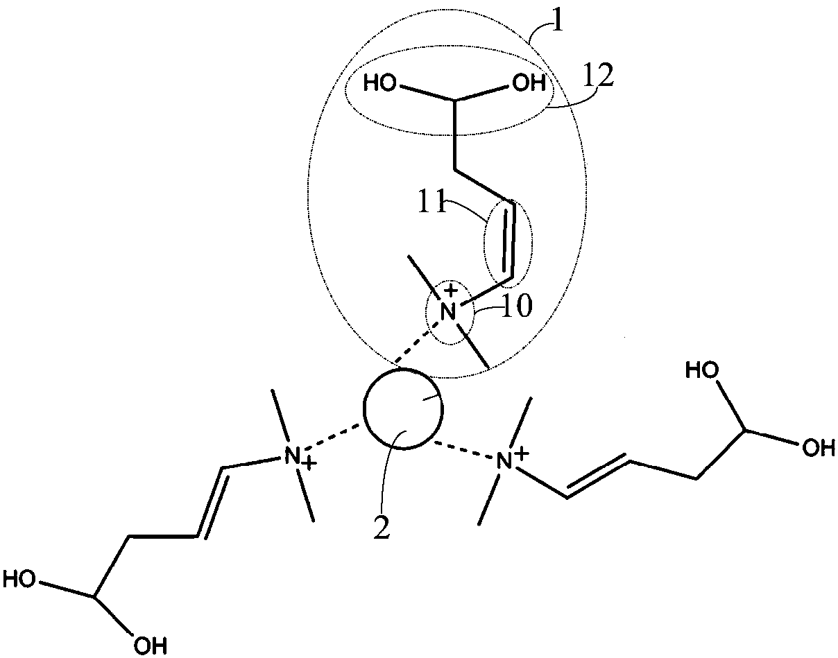
[0033] This embodiment provides a kind of zinc oxide ink, such as figure 1 As shown, it includes zinc oxide nanoparticles 2 loaded with a ligand 1, and the ligand 1 adopts an aliphatic chain with more than two carbon atoms; the ligand 1 has a crosslinkable group 11 on the side close to the coordination atom 10.
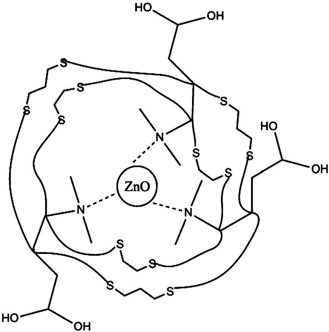
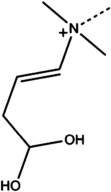
[0034] In this embodiment, the ligand 1 adopts an alcohol amine aliphatic chain with three to eight carbons. By making the zinc oxide nanoparticles 2 adopt the ligand 1 whose chain length is greater than two carbon atoms, compared with the zinc oxide nanoparticles whose ligand is ethanolamine (that is, the ligand chain length is two carbon atoms) in the prior art, increase The steric hindrance between the zinc oxide nanoparticles 2 is avoided, thereby avoiding the aggregation between the zinc oxide nanoparticles 2, and further avoiding the formation of black spots in the film layer formed by using the zinc oxide ink. The crosslinkable group 11 can make self-crosslink...
Embodiment 2
[0053] This embodiment provides an electron transport film layer, which is formed by using the zinc oxide ink in Embodiment 1.
[0054] Wherein, the electron transport film layer can be used as an electron transport layer in an organic electroluminescent device. Zinc oxide ink forms the electron transport film layer by inkjet printing, and its specific preparation method is:
[0055] When the electron transport film layer is formed by printing the zinc oxide ink containing a crosslinkable group in the ligand, the zinc oxide ink is printed on the substrate by inkjet printing, and the substrate loaded with the zinc oxide ink is exposed to ultraviolet light. (Wavelength 365nm) irradiation for about 5 minutes, after the completion of the vacuum degree of 500mbar, heating at 50 degrees for about half an hour to prepare a dense zinc oxide film layer.
[0056] When using zinc oxide ink containing two cross-linkable groups in the ligand to print to form the electron transport film la...
Embodiment 3
[0059] This embodiment provides a display device, including the electron transport film layer in Embodiment 2. The display device is an organic electroluminescence display device.
[0060] By using the electron transport film layer in Example 2, the quality of the display device is improved.
[0061] The display device provided by the present invention can be any product or component with a display function such as an OLED panel, a QLED panel, an OLED TV, a QLED TV, a monitor, a mobile phone, or a navigator.
PUM
 Abstract
Description
Claims
Application Information
 - Generate Ideas
- Intellectual Property
- Life Sciences
- Materials
- Tech Scout
- Unparalleled Data Quality
- Higher Quality Content
- 60% Fewer Hallucinations
Browse by: Latest US Patents, China's latest patents, Technical Efficacy Thesaurus, Application Domain, Technology Topic, Popular Technical Reports.
© 2025 PatSnap. All rights reserved.Legal|Privacy policy|Modern Slavery Act Transparency Statement|Sitemap|About US| Contact US: help@patsnap.com


