Forming method for fin-type field effect transistor

A fin-type field effect transistor and fin technology are applied in the direction of electrical components, semiconductor/solid-state device manufacturing, circuits, etc., to achieve the effect of improving electrical performance and good performance

Active Publication Date: 2018-01-16
SEMICON MFG INT (SHANGHAI) CORP +1
View PDF6 Cites 1 Cited by
  • Summary
  • Abstract
  • Description
  • Claims
  • Application Information

AI Technical Summary

Problems solved by technology

[0005] However, the performance of the fin field effect transistor formed by the prior art needs to be further improved

Method used


Image

  • Forming method for fin-type field effect transistor
  • Forming method for fin-type field effect transistor
  • Forming method for fin-type field effect transistor

Examples


Embodiment Construction

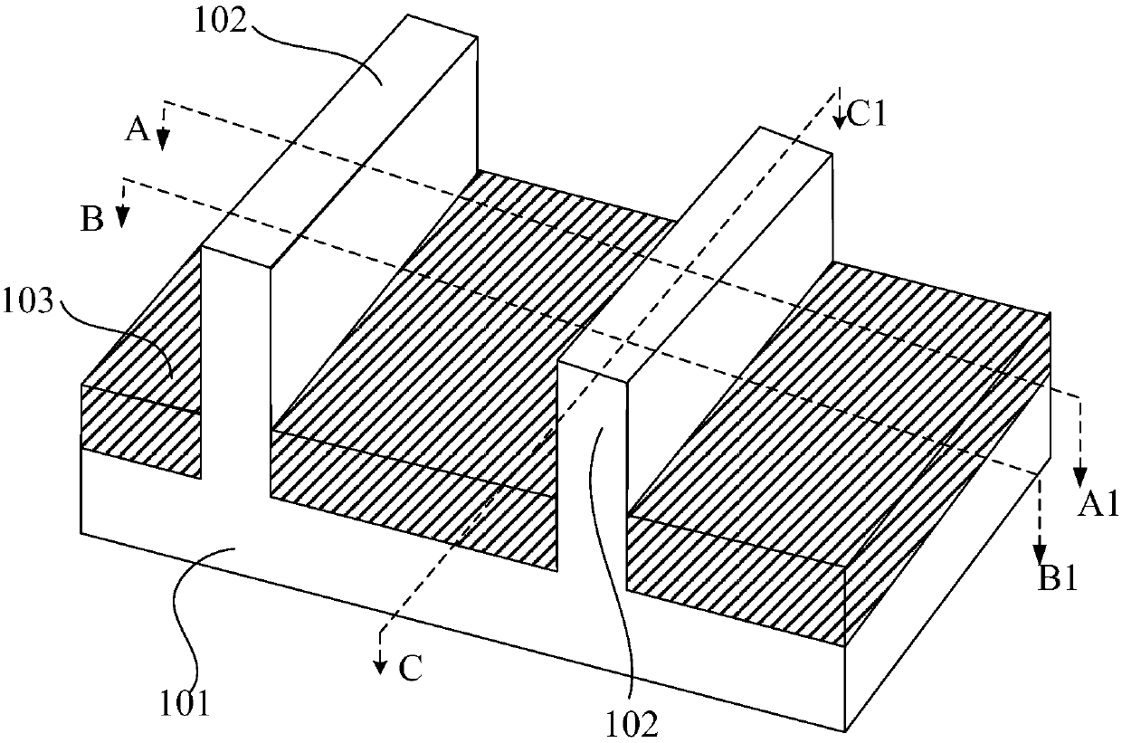
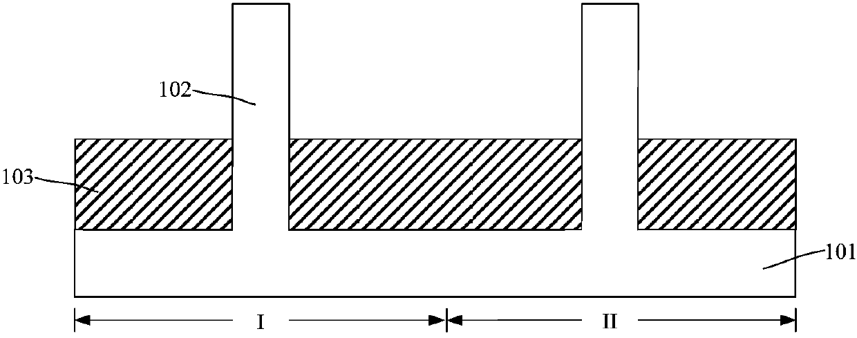
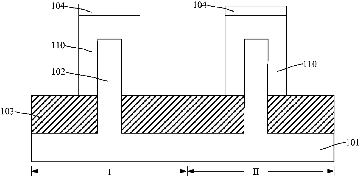
[0032] It can be seen from the background art that the performance of the fin field effect transistor formed in the prior art needs to be further improved, especially the electrical performance of the NMOS fin field effect transistor is poor.

[0033] According to the analysis, the formation process of the NMOS fin field effect transistor includes the steps of: forming a mask side wall on the side wall of the fin in the NMOS region; Forming an N-region groove in the portion; forming an N-type doped epitaxial layer filling the N-region groove. In order to limit the shape and volume of the formed N-region doped epitaxial layer, when etching and removing the fins with partial thickness on both sides of the gate structure in the NMOS region, the mask sidewalls located on the sidewalls of the fins are kept, so that the formed The two opposite sidewalls of the groove in the N region are mask sidewalls; during the process of forming the N-type doped epitaxial layer, the mask sidewall...


PUM


Abstract

The invention discloses a forming method for a fin-type field effect transistor, and the method comprises the steps: forming an N-region mask side wall on side walls of fin parts in an NMOS region; forming a supporting layer, which is closely attached to the side wall of the N-region mask side wall, on an isolated structure; removing a part of the fin parts at two sides of a grid structure of theNMOS region through etching, wherein the fin parts of the NMOS region and the N-region mask side wall form an N-region groove through enclosing; removing the supporting layer after the forming of theN-region groove; and forming an N-type doped epitaxial layer which is filled in the N-region groove. According to the invention, the supporting layer achieves the supporting of the N-region mask sidewall, prevents the N-region mask side wall from collapsing, and improves the performance of the formed fin-type field effect transistor.

Description

technical field [0001] The invention relates to the technical field of semiconductor manufacturing, in particular to a method for forming a fin field effect transistor. Background technique [0002] With the continuous development of semiconductor process technology, the development trend of semiconductor process nodes following Moore's Law continues to decrease. In order to adapt to the reduction of process nodes, the channel length of MOSFET field effect transistors has to be continuously shortened. The shortening of the channel length has the advantages of increasing the die density of the chip and increasing the switching speed of the MOSFET field effect tube. [0003] However, as the channel length of the device is shortened, the distance between the source and the drain of the device is also shortened, so that the control ability of the gate to the channel becomes worse, and the gate voltage pinches off the channel. The difficulty is also increasing, making the pheno...

Claims


Application Information

Patent Timeline
IPC IPC(8): H01L21/336
Inventor 李勇
Owner SEMICON MFG INT (SHANGHAI) CORP
Why Eureka
Try Eureka