Measurement method of trap energy level distribution in oxide layer of semiconductor device
A trap energy level, oxide layer technology, applied in the direction of single semiconductor device testing, non-contact testing, etc., can solve the problems of poor conductivity, difficulty in characterizing traps in the silicon dioxide layer, and low carrier concentration, and achieve simple steps. Effect
- Summary
- Abstract
- Description
- Claims
- Application Information
AI Technical Summary
Problems solved by technology
Method used
Image
Examples
Embodiment Construction
[0028] The method for measuring the energy level of traps in the oxide layer of a semiconductor device according to the present invention will be described in detail below in conjunction with the accompanying drawings. Taking the p-channel MOS transistor as an example, the oxide layer of the device is prepared by dry oxidation at 900°C, with a thickness of 80 nanometers:
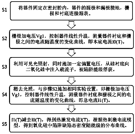
[0029] figure 1 It is a test flowchart of the present invention, comprising the following steps:
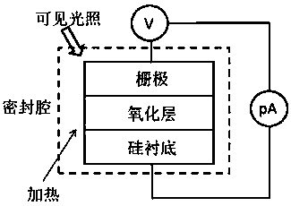
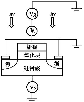
[0030] Step S1, fix the device in the sealed cavity, such as figure 2 As shown, the source and drain of the device are grounded, and the substrate and gate are connected to the source meter HP4140B to apply voltage and measure current.
[0031] In step S2, in the absence of carrier injection, a bias voltage of -10V is applied between the gate and the substrate, and the temperature of the device in the sealed cavity is controlled to rise linearly at a rate of 0.1°C / min from room temperature of 25°C. Until 35...
PUM
 Abstract
Description
Claims
Application Information
 - R&D Engineer
- R&D Manager
- IP Professional
- Industry Leading Data Capabilities
- Powerful AI technology
- Patent DNA Extraction
Browse by: Latest US Patents, China's latest patents, Technical Efficacy Thesaurus, Application Domain, Technology Topic, Popular Technical Reports.
© 2024 PatSnap. All rights reserved.Legal|Privacy policy|Modern Slavery Act Transparency Statement|Sitemap|About US| Contact US: help@patsnap.com


