Silicon carbide Trench MOS device and manufacturing method thereof

A manufacturing method and technology of silicon carbide, applied in semiconductor/solid-state device manufacturing, semiconductor devices, electrical components, etc., can solve the problems of low work efficiency, high power loss, and high production cost

Active Publication Date: 2017-12-01
HANGZHOU SILICON-MAGIC SEMICON TECH CO LTD
View PDF4 Cites 8 Cited by
  • Summary
  • Abstract
  • Description
  • Claims
  • Application Information

AI Technical Summary

Problems solved by technology

The present invention adds a layer of polysilicon with π-type distribution under the trench gate structure of the traditional device to form a heterojunction with the epitaxial layer; using the silicon

Method used


Image

  • Silicon carbide Trench MOS device and manufacturing method thereof
  • Silicon carbide Trench MOS device and manufacturing method thereof
  • Silicon carbide Trench MOS device and manufacturing method thereof

Examples


Embodiment 1

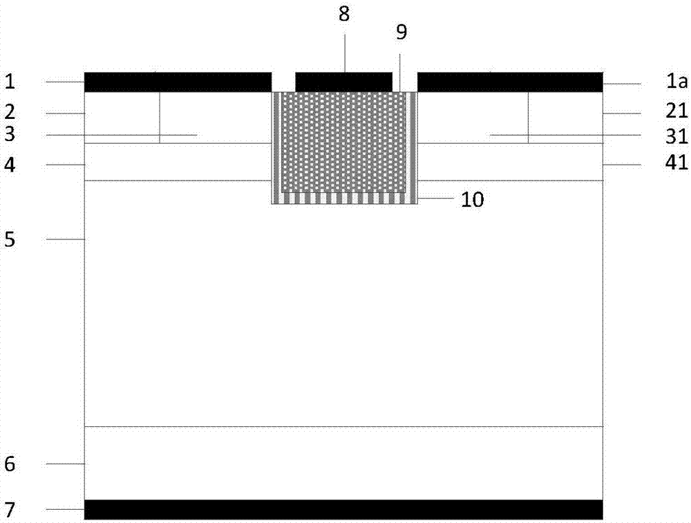
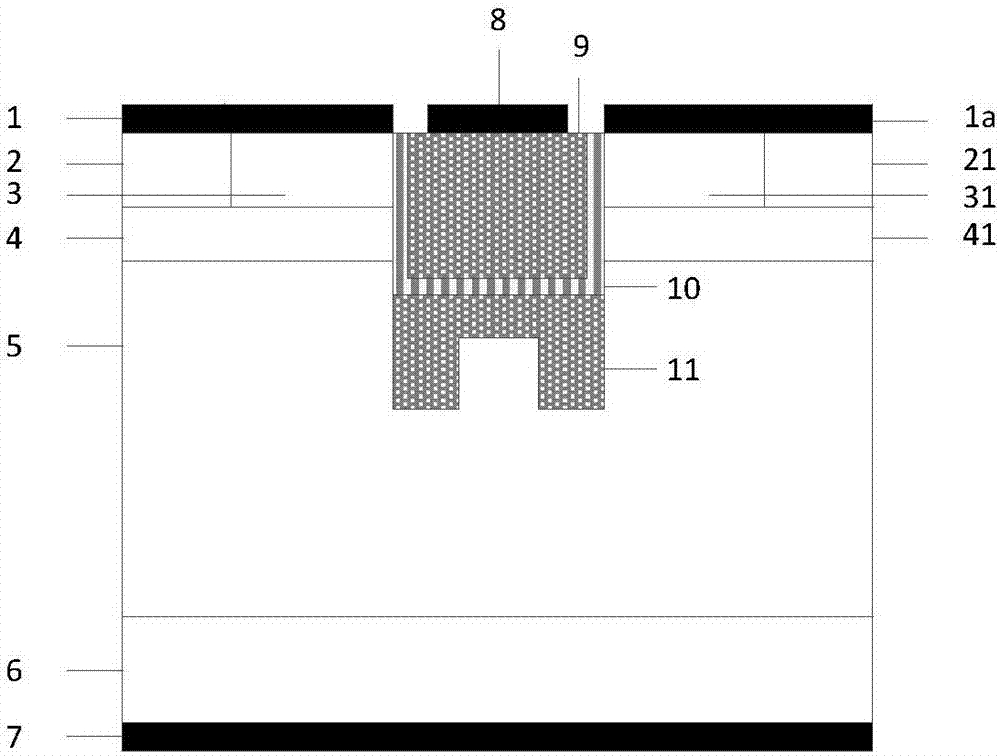
[0109] A silicon carbide Trench MOS device, its cell structure is as follows figure 2 Shown includes: metal drain electrodes 7, N + Substrate 6 and N - epitaxial layer 5; the N - One end of the upper layer of the epitaxial layer 5 has a first Pbase region 4, the N - The other end of the upper layer of the epitaxial layer 5 has a second Pbase region 41; the first Pbase region 4 has mutually independent first N + source region 3 and the first P + Contact region 2; the second Pbase region 41 has second N independent of each other + source region 31 and the second P + Contact area 21; the first P + contact zone 2 and the first N + The upper surface of the source region 3 has a first metal source electrode 1; the second P + contact region 21 and the second N + The upper surface of the source region 31 has a second metal source electrode 1a; it is characterized in that: there is a P-type polysilicon region 11 with a π-type distribution in the N-epitaxial layer 5 below the m...

Embodiment 2

[0112] In this embodiment, independent first P + SiC region 12 and the second P + Except for the silicon carbide region 121, all the other structures are the same as in Embodiment 1, such as image 3 Shown; the first P in this embodiment + SiC region 12 and the second P + The width of the silicon carbide region 121 is the same as that of the corresponding branch region, and the width is 0.1-0.3 μm.

[0113] Compared with Example 1, the two P introduced in this example + The silicon carbide regions 12 and 121 can shield the P-type polysilicon region 11 and the trench gate thereon from the electric field, improve the withstand voltage of the device, and reduce the reverse leakage current.

Embodiment 3

[0115] In addition to making the first P + SiC region 12 and the second P + Except that the width of the silicon carbide region 121 is greater than the width of the corresponding branch region of the P-type polysilicon region 11 in the π-type distribution, the rest of the structure is the same as that of Embodiment 2, as Figure 4 shown.

[0116] In this example, the first P + SiC region 12 and the second P + The width of the silicon carbide region 121 is 0.1-0.4 μm.

[0117] This implementation will P + The larger lateral dimensions of the silicon carbide regions 12 and 121 can enable the P-type polysilicon region 11 to have a stronger electric field shielding effect, further improve the withstand voltage capability of the device, and reduce the reverse leakage current.


PUM

PropertyMeasurementUnit
Thicknessaaaaaaaaaa
Doping concentrationaaaaaaaaaa
Thicknessaaaaaaaaaa

Abstract

The invention discloses a silicon carbide Trench MOS device and a manufacturing method thereof, and belongs to the technical field of power semiconductors. The method includes: a layer of a polysilicon region distributed in a pi shape is additionally arranged under a trench gate structure of a conventional device, the polysilicon region and an epitaxial layer form a Si/SiC heterojunction, and a diode is integrated in the device. Compared with a parasitic silicon carbide diode which directly employs a silicon carbide Trench MOS, according to the silicon carbide Trench MOS device and the manufacturing method thereof, the junction voltage drop of the device diode during application is substantially reduced, and the switch-on characteristic of the device is improved through large junction area of the heterojunction; moreover, the gate-drain capacitance and the ratio of the gate-drain capacitance to the gate-source capacitance of the device are reduced, and the performance and the reliability of the device MOS during application are enhanced; besides, the silicon carbide Trench MOS device and the manufacturing method thereof are also advantageous in that the reverse recovery time is short, the reverse recovery charges are less, and advantages including low reverse leakage, high breakdown voltage, and good temperature stabilization performance of the conventional silicon carbide Trench MOS device are maintained. In conclusion, according to the silicon carbide Trench MOS device and the manufacturing method thereof, the prospect is wide in circuits such as inversion circuits and chopper circuits etc.

Description

technical field [0001] The invention belongs to the technical field of power semiconductors, and in particular relates to a silicon carbide Trench MOS device and a manufacturing method thereof. Background technique [0002] Since the beginning of the 21st century, many forms of new energy have emerged, such as wind energy, nuclear energy, solar energy, and geothermal energy. occupy an absolute advantage in energy consumption. But it is undeniable that the large-scale and long-term use of fossil energy will inevitably lead to a series of environmental and social problems, and these problems are also closely related to the current global warming and other global environmental degradation issues. In order to achieve high-efficiency use of energy resources and sustainable development, converting fossil energy into electric energy to improve its use efficiency has become one of the important solutions to the world's energy problems. [0003] The power system is a necessary way ...

Claims


Application Information

Patent Timeline
IPC IPC(8): H01L29/78H01L29/423H01L29/06H01L29/12H01L21/336
CPCH01L29/0615H01L29/0684H01L29/1604H01L29/4236H01L29/66477H01L29/7831
Inventor 张金平邹华刘竞秀李泽宏任敏张波
Owner HANGZHOU SILICON-MAGIC SEMICON TECH CO LTD
Why Eureka
Try Eureka