Circuit board punching mold and punching method thereof

A board stamping and mold technology, which is applied in the field of circuit board stamping dies and stamping molds, can solve the problems of insufficient impact tonnage, high hardness, and large damage to the shape of rigid circuit boards.

Pending Publication Date: 2017-11-28
惠州市永隆电路有限公司
View PDF8 Cites 0 Cited by
  • Summary
  • Abstract
  • Description
  • Claims
  • Application Information

AI Technical Summary

Problems solved by technology

The mold punching process also has its own weaknesses, because the rigid circuit board is thick and hard
The impact tonnage (impulse force) of the conventional mold punching type is not enough, and the damage to the shape of the rigid circuit board is large
Affect appearance and dimensional accuracy
The cost of punch dies with super large tonnage is also very high

Method used


Image

  • Circuit board punching mold and punching method thereof
  • Circuit board punching mold and punching method thereof

Examples


Embodiment 1

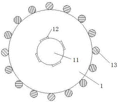
[0023] A circuit board stamping die, comprising a body 1, characterized in that the center of the body 1 is provided with a protrusion 11, and the protrusion 11 is symmetrically provided with reinforcing ribs 12; the edge of the body 1 is symmetrically provided with an estimation portion 13 , the estimation part 13 is higher than the body 11-10mm, and the body 1 is integrally connected with the estimation part 13 .

[0024] Further, the body 1 is in the shape of a round cake.

[0025] Further, the estimation part 13 is a cylinder. The diameter of the estimation part 13 is 0.5-2 mm. The horizontal distance between the adjacent estimation parts 13 is 10-20 mm.

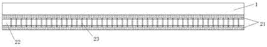
[0026] Further, a buffer portion is provided under the body 1 , the buffer portion includes a first buffer layer 21 and a second buffer layer 22 , and the first buffer layer 21 is symmetrically arranged at both ends of the second buffer layer 22 .

[0027] Further, the first buffer layer 21 is a polymer hydrogel layer...


PUM

PropertyMeasurementUnit
Diameteraaaaaaaaaa

Abstract

The invention provides a circuit board punching mold and a punching method thereof. The circuit board punching mold comprises a body, and is characterized in that a boss is arranged at the center of the body, and the boss is symmetrically provided with reinforcing ribs; the edge of the body is symmetrically provided with pushing and fixing parts which are higher than the body by 1-10 mm; and the body is integrally connected with the pushing and fixing parts. By means of circuit board cooperation of relatively densely-distributed force unloading holes drilled in advance, and then by means of the pushing and fixing parts designed on the mold punching edge, about 1 / 3 impacting area of the mold is reduced; because of reduction of the stress area, the pressure intensity of the mold on a hard circuit board is increased; and by means of cooperation with the force unloading holes of the circuit board, the cohesion resultant force originally formed because glass fiber cloth is buckled silk by silk is cut off and disorganized roughly, and the offsetting force on the mold caused by the strength of the hard circuit board is weakened.

Description

technical field [0001] The invention relates to the technical field of circuit board processing, in particular to a circuit board stamping die and a stamping method thereof. Background technique [0002] With the development of the electronics industry towards refinement, many rigid circuit boards tend to use the milling process to process the shape. Due to the high-speed cutting with milling cutters, they generally have smooth and delicate characteristics. However, compared with the early mold stamping of rigid circuit boards, it also has disadvantages, such as high cost and long production hours. [0003] Due to the rapid development of the circuit board industry, the profit is getting thinner and thinner, especially for low-end and simple products, the profit is even lower. Companies are having to think of ways to consider cost-saving solutions. Low-end and simple products are often accompanied by mass production, which is more suitable for punching with molds to save...

Claims


Application Information

Patent Timeline
IPC IPC(8): B26F1/44B26F1/14B26D7/00
CPCB26D7/00B26F1/14B26F1/44B26F2210/08
Inventor 叶钢华吴永强肖长林彭遥
Owner 惠州市永隆电路有限公司
Why Eureka
Try Eureka