Double-sided cooling power module based on multi-area parallel arrangement
A double-sided heat dissipation, power module technology, applied in electrical components, electrical solid devices, circuits, etc., can solve the problems of hindering power density, chip overvoltage breakdown, parasitic inductance difficulty, etc., to reduce the area of the commutation loop, The effect of increasing the area of the metal layer and reducing the lead resistance
- Summary
- Abstract
- Description
- Claims
- Application Information
AI Technical Summary
Problems solved by technology
Method used
Image
Examples
Embodiment 1
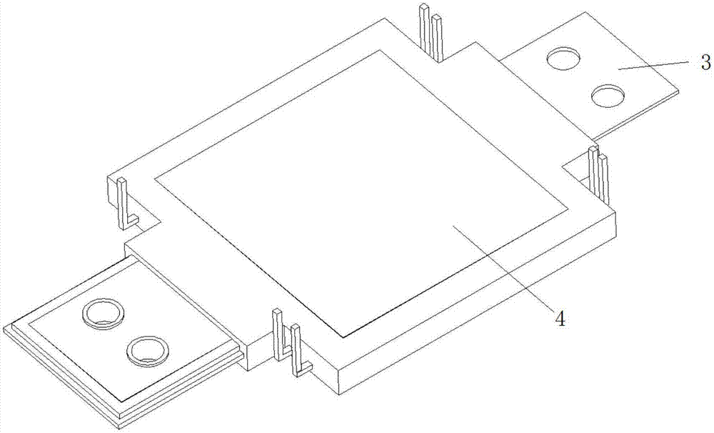
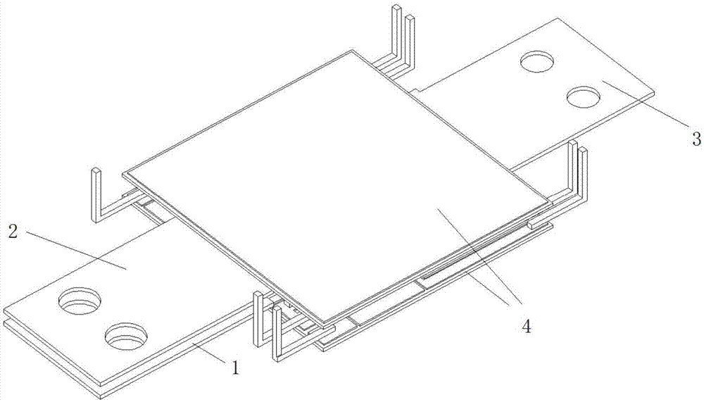
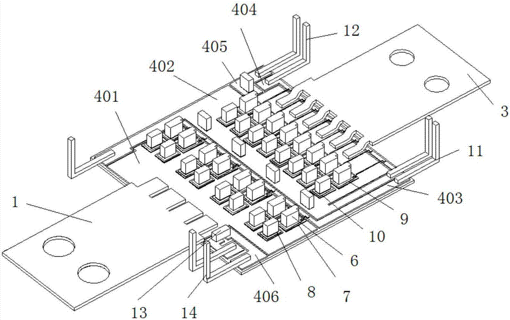
[0029] like figure 1 As shown, a double-sided heat dissipation power module arranged side by side in multiple areas includes a positive power terminal 1, a negative power terminal 2 and an output power terminal 3, and each of the positive power terminal 1 and the negative power terminal 2 is connected to a metal insulating substrate 4, Two metal insulating substrates 4 are stacked. It can be seen in the figure that the metal insulating substrate 4 on the top is connected to the negative power terminal 2 , and the metal insulating substrate 4 on the bottom is connected to the positive power terminal 1 . An upper half-bridge chip and a lower half-bridge chip are sintered on the metal insulating substrate 4 connected to the positive power terminal 1 , and both the upper half-bridge chip and the lower half-bridge chip are connected to the opposite metal layer through a metal block 6 .
[0030] The positive power terminal 1 and the negative power terminal 2 are stacked, and the con...
Embodiment 2
[0039] like Figure 9 , Figure 10 As shown, the structure of this embodiment is basically the same as that of Embodiment 1, the difference is that in this embodiment, the metal insulating substrate 4 connected to the positive power terminal 1 is provided with an annular insulating groove 5, and the ring-shaped insulating groove 5 surrounds A lower half-bridge chip is sintered on the metal layer, and the metal layer outside the annular insulating groove 5 is connected to the output power terminal 3 through a metal block, and an upper half-bridge chip is sintered on it;
[0040] The metal insulating substrate 4 connected to the positive power terminal 1 is provided with a second positive metal layer 411, a second negative metal layer 412 surrounded by an annular insulating groove 5, a second upper half bridge gate metal layer 413 and a second lower half bridge. The bridge gate metal layer 414; the positive power terminal 1 and the upper half-bridge chip are sintered on the sec...
PUM
 Abstract
Description
Claims
Application Information
 - R&D
- Intellectual Property
- Life Sciences
- Materials
- Tech Scout
- Unparalleled Data Quality
- Higher Quality Content
- 60% Fewer Hallucinations
Browse by: Latest US Patents, China's latest patents, Technical Efficacy Thesaurus, Application Domain, Technology Topic, Popular Technical Reports.
© 2025 PatSnap. All rights reserved.Legal|Privacy policy|Modern Slavery Act Transparency Statement|Sitemap|About US| Contact US: help@patsnap.com


