Diode and power convertor using the same
A technology of diodes and cathode electrodes, which is applied in the direction of output power conversion devices, diodes, and conversion of AC power input to DC power output. The effect of reducing the conduction loss and reducing the leakage current
- Summary
- Abstract
- Description
- Claims
- Application Information
AI Technical Summary
Problems solved by technology
Method used
Image

Examples
no. 1 approach 》
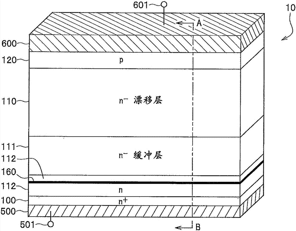
[0071] The diode 10 according to the first embodiment of the present invention will be described with reference to the drawings.
[0072] "Outline of Structure of Diode 10"
[0073] figure 1 An example of the upper surface and the cross section of the diode 10 according to the first embodiment of the present invention is shown.
[0074] exist figure 1 Among them, the diode 10 is formed between the anode electrode layer 600 to which the anode electrode 601 is connected and the cathode electrode layer 500 to which the cathode electrode 501 is connected.
[0075] In addition, the anode electrode layer 600 and the cathode electrode layer 500 are layers mainly made of metal.
[0076] The anode electrode layer 600 is in contact with the upper surface (the upper surface of the paper surface) of the p-type semiconductor layer 120 (the second semiconductor layer of the second conductivity type).
[0077] The lower surface of the p-type semiconductor layer 120 is connected to the n ...
no. 1 approach
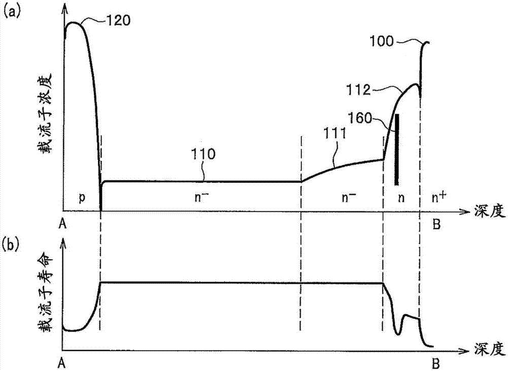
[0144] - buffer layer>
[0145] In addition, the inventors of the present invention confirmed the effect of reducing the leakage current at the time of reverse voltage blocking as an effect of the buffer layer structure with respect to the low-injection structure of the cathode.
[0146] Figure 19 An example of leakage current characteristics at the time of reverse voltage blocking using the diode 10 according to the first embodiment of the present invention is shown. In addition, as a comparison, characteristic examples of the prior art are also shown together.
[0147] exist Figure 19 , the horizontal axis represents the voltage (Vka) between the anode and cathode of the diode, and the vertical axis represents the anode current (Ia) in natural logarithm. In addition, characteristic line 191 ( 191A, 191B) is a characteristic of diode 10 according to the first embodiment of the present invention, and characteristic line 192 ( 192A, 192B) is a characteristic example of a c...
no. 2 approach 》
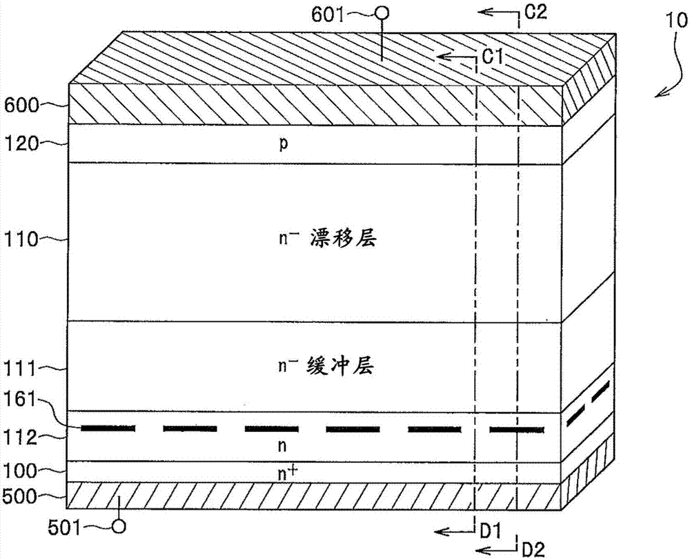
[0156] A diode 10 according to a second embodiment of the present invention will be described with reference to the drawings.
[0157] image 3 An example of the upper surface and cross section of the diode 10 according to the second embodiment of the present invention is shown.
[0158] exist image 3 in, with figure 1 The difference is the configuration of the low carrier lifetime control layer 161 .
[0159] The low carrier lifetime control layer 161 is partially formed in the shallow n buffer layer 112 . For example, in image 3 At C2-D2 representing the position of the cross section, the low carrier lifetime control layer 161 and figure 1 The low carrier lifetime control layer 160 in the same exists, but in image 3 The C1-D1 that indicates the cross-section position does not exist.
[0160] Figure 4 represents the diode 10 of the second embodiment of the present invention image 3 Examples of depth-direction cross-sectional profiles in the C1-D1 cross-section a...
PUM
 Abstract
Description
Claims
Application Information
 - R&D
- Intellectual Property
- Life Sciences
- Materials
- Tech Scout
- Unparalleled Data Quality
- Higher Quality Content
- 60% Fewer Hallucinations
Browse by: Latest US Patents, China's latest patents, Technical Efficacy Thesaurus, Application Domain, Technology Topic, Popular Technical Reports.
© 2025 PatSnap. All rights reserved.Legal|Privacy policy|Modern Slavery Act Transparency Statement|Sitemap|About US| Contact US: help@patsnap.com