ETFE (ethylene-tetrafluoroethylene copolymer) film and preparation method thereof
A thin film and additive technology, which is applied in the field of ETFE thin film and its preparation, can solve the problems that thin film technology is difficult to master, and achieve the effects of strong practical value, super insulation and low thermal resistance
- Summary
- Abstract
- Description
- Claims
- Application Information
AI Technical Summary
Problems solved by technology
Method used
Image
Examples
Embodiment 1
[0025] The following raw materials are calculated in parts by weight:
[0026] 100 parts of ETFE;
[0027] 10 parts of PFA;
[0028] 0.5 parts of graphene;
[0029] Among them, the melt index of ETFE is 20.
[0030] Step 1, add above-mentioned ETFE, PFA, graphene to high mixer and fully mix;
[0031] Step 2, granulating the above-mentioned mixture to make granules;
[0032] Step 3, adding the above granules to a screw extruder, heating to 190-210°C, melting and extruding, forming a film through a flat mold;
[0033] Step 4, cooling the formed film at 90-100°C by a cooling roller, and drying in vacuum;
[0034] Step 6, trimming and winding to obtain the ETFE film.
[0035] The film product has a thickness of 50 μm, a width of 550 mm, a transparent color and a bright surface.
Embodiment 2
[0037] The following raw materials are calculated in parts by weight:
[0038] 100 parts of ETFE;
[0039] 10 parts of PFA;
[0040] PVDF 10 parts;
[0041] PMMA 10 parts;
[0042] 2.5 parts of graphene;
[0043] Among them, the melt index of ETFE is 25.
[0044] Weigh the raw materials of the above formula, and make a film according to the method described in Example 1; the film product has a thickness of 50 μm, a width of 550 mm, a transparent color, and a bright surface, which can be used as a semiconductor release film.
Embodiment 3
[0046] The following raw materials are calculated in parts by weight:
[0047] 100 parts of ETFE;
[0048] PMMA 10 parts;
[0049] 2 parts of graphene;
[0050] Among them, the melt index of ETFE is 22.
[0051] Weigh the raw materials of the above formula, and make a film according to the method described in Example 1; the film product has a thickness of 50 μm, a width of 550 mm, and a transparent color.
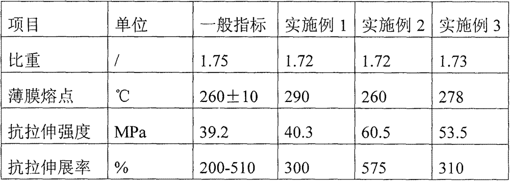
[0052] Table 1: Basic properties of the film products obtained in the above-mentioned embodiments 1-3
[0053]
[0054]
PUM
| Property | Measurement | Unit |
|---|---|---|
| Thickness | aaaaa | aaaaa |
| Width | aaaaa | aaaaa |
Abstract
Description
Claims
Application Information
 - Generate Ideas
- Intellectual Property
- Life Sciences
- Materials
- Tech Scout
- Unparalleled Data Quality
- Higher Quality Content
- 60% Fewer Hallucinations
Browse by: Latest US Patents, China's latest patents, Technical Efficacy Thesaurus, Application Domain, Technology Topic, Popular Technical Reports.
© 2025 PatSnap. All rights reserved.Legal|Privacy policy|Modern Slavery Act Transparency Statement|Sitemap|About US| Contact US: help@patsnap.com


