Dielectric films and electronic components

A dielectric film, X-ray technology, applied in fixed capacitor parts, fixed capacitor dielectrics, electrical components, etc., can solve the problem of difficult to respond to miniaturization requirements, and achieve high Q value, high relative permittivity, high The effect of insulation breakdown voltage

Active Publication Date: 2019-12-06
TDK CORPARATION
View PDF1 Cites 0 Cited by
  • Summary
  • Abstract
  • Description
  • Claims
  • Application Information

AI Technical Summary

Problems solved by technology

[0005] For example, because the Q value of amorphous SiNx film is as high as about 500 at high frequency (2 GHz), the insulation breakdown voltage is also as high as 500V / μm to 700V / μm, so it is widely used in electronic components corresponding to high frequency. However, since the relative permittivity is as low as about 7, a large electrode area is required to achieve the target function, and it is difficult to respond to the demand for miniaturization.

Method used


Image

  • Dielectric films and electronic components
  • Dielectric films and electronic components
  • Dielectric films and electronic components

Examples


Embodiment 1>< comparative example 1

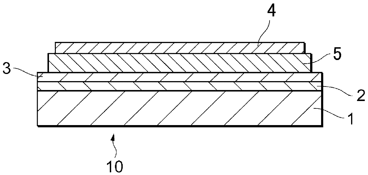
[0063] First, 6 μm thick SiO on the surface of 350 μm thick Si 2 On the surface of the 10 mm×10 mm square support substrate of the insulating layer, a Cr thin film as an underlayer was formed so as to have a thickness of 20 nm by a sputtering method.

[0064] Next, on the base layer of the Cr thin film formed above, a Cu thin film as a lower electrode was formed by sputtering so as to have a thickness of 100 nm.

[0065] For the formed Cr / Cu thin film, the heating rate is set to 10°C / min, the holding temperature is set to 150°C, the temperature holding time is set to 0.5 hours, and the atmosphere is set to a nitrogen atmosphere. Carry out heat treatment.

[0066] A sputtering method was used for the formation of the dielectric film. The target required for forming the dielectric film was produced as follows.

[0067]First, MgCO was carried out so that the amounts of Mg, Ca, Sr, Ba, Ta, Nb, V, Hf, Zr, Ti, and Zn in Sample No. 1 to Sample No. 47 shown in Table 1 were obtained...

Embodiment 2

[0101] Except for changing the thickness of the dielectric film, a sample was prepared in the same manner as in Example 1, Sample No. 29, and the same evaluation as in Example 1 was performed. The results are shown in Table 3.

[0102] [table 3]

[0103]

[0104] Sample No.48~Sample No.50

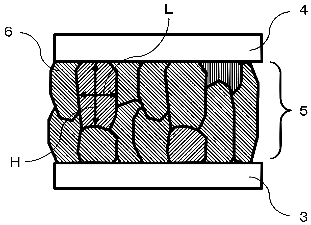
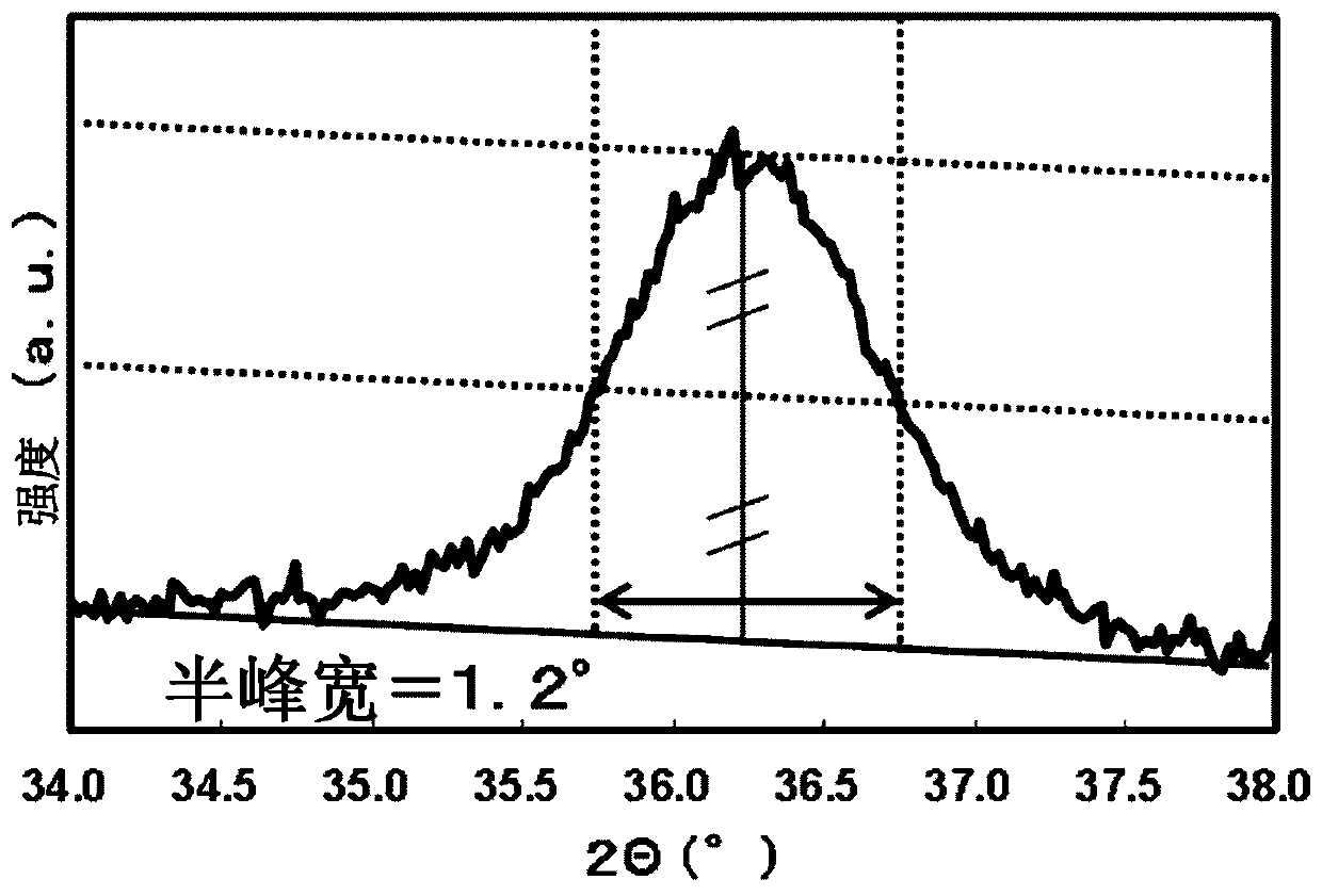
[0105] From Table 3, it can be confirmed that even if the film thickness of the dielectric film is different, as long as the dielectric film has an alkaline earth metal oxide having a NaCl-type crystal structure as the main component, and the dielectric film has a (111) orientation in the normal direction In the Cu-Kα X-ray diffraction pattern of the above-mentioned dielectric film, the characteristic dielectric film with a half width of the diffraction peak (111) of 0.3° to 2.0° exhibits substantially the same characteristics even when the film is thinned to 50 nm. . That is, it was confirmed that as long as the dielectric film has the characteristics of the present invention, even i...


PUM

PropertyMeasurementUnit
thicknessaaaaaaaaaa
thicknessaaaaaaaaaa
thicknessaaaaaaaaaa

Abstract

An object of the present invention is to provide a dielectric film having a high relative permittivity, Q value, and dielectric breakdown voltage, and an electronic component using the dielectric composition. The dielectric film is characterized in that the dielectric film is mainly composed of an alkaline earth metal oxide having a NaCl-type crystal structure, the dielectric film has a columnar structure with (111) orientation in the normal direction, and the dielectric film has a In the Cu-Kα X-ray diffraction diagram, the half-maximum width of the diffraction peak of (111) is 0.3°-2.0°.

Description

technical field [0001] The present invention relates to a dielectric film and an electronic component. Background technique [0002] In response to the further high-speed and large-capacity communication of mobile communication devices represented by smartphones and tablet PCs, the practical use of MIMO technology (Multi-Input Multi-Output) using multiple frequency bands at the same time has begun. As the frequency band used for communication increases, individual high-frequency components are required for each frequency band, and the number of components is increased to maintain the size of the device, and further miniaturization and higher functionality of each component are required. [0003] Examples of electronic components corresponding to such high frequencies include duplexers, bandpass filters, and the like. These are all composed of a combination of a dielectric that acts as a capacitance and a magnetic body that acts as an inductance, but in order to obtain good ...

Claims


Application Information

Patent Timeline
Patent Type & Authority Patents(China)
IPC IPC(8): H01G4/12C04B35/495H01B3/12
CPCC04B35/495H01B3/12H01G4/1209H01G4/085H01G4/1227H01L21/02175H01L21/02194H01L21/02266C04B2235/3205H01L28/55C04B35/01C04B2235/787C04B35/03C04B35/04C04B35/057C04B35/62218C04B2235/3206C04B2235/3208C04B2235/3213C04B2235/3215C04B2235/3239C04B2235/3244C04B2235/3255C04B2235/3284C04B2235/762H01G4/10H01G4/33H01G4/30C01F5/02C01F11/02C01P2002/74C04B2235/3236C04B2235/3248C23C14/082C23C14/185C23C14/3414C04B35/486
Inventor 内山弘基政冈雷太郎藤井祥平城川真生子
Owner TDK CORPARATION
Why Eureka
Try Eureka