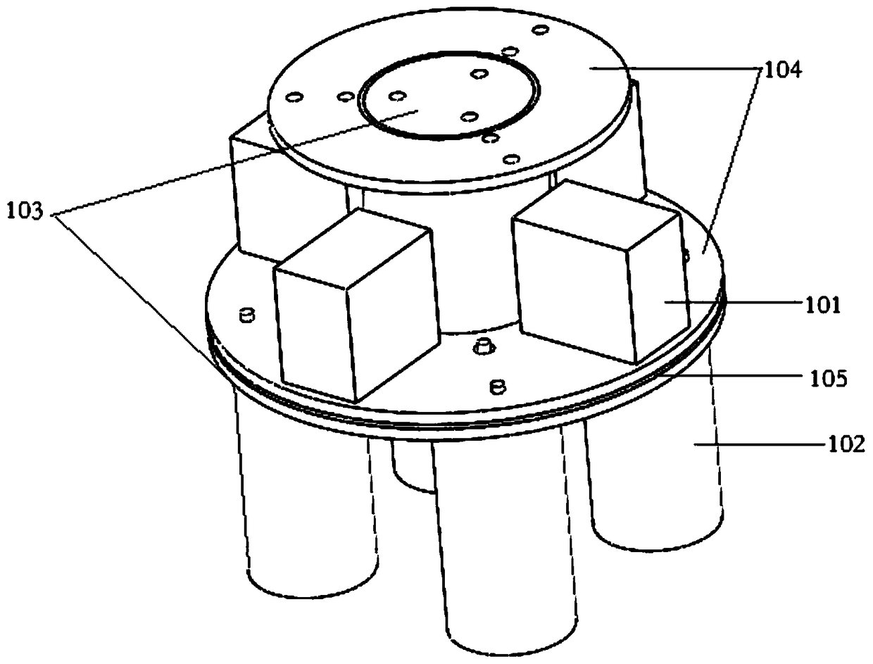
A DC busbar

A technology of DC busbars, together, applied in output power conversion devices, climate sustainability, high-efficiency power electronic conversion, etc., can solve problems such as drain-source voltage overshoot, reduce parasitic inductance, and solve leakage-source Effect of pole voltage overshoot and length reduction

Active Publication Date: 2019-02-12
NORTH CHINA ELECTRIC POWER UNIV (BAODING)
View PDF7 Cites 0 Cited by
  • Summary
  • Abstract
  • Description
  • Claims
  • Application Information

AI Technical Summary

Problems solved by technology

[0004] The purpose of the present invention is to provide a new type of DC busbar to solve the problem of drain-source voltage overshoot during the turn-off process of silicon carbide power MOSFET devices

Method used


Image

  • A DC busbar
  • A DC busbar
  • A DC busbar

Examples


Embodiment Construction

[0049] The following will clearly and completely describe the technical solutions in the embodiments of the present invention with reference to the accompanying drawings in the embodiments of the present invention. Obviously, the described embodiments are only some, not all, embodiments of the present invention. Based on the embodiments of the present invention, all other embodiments obtained by persons of ordinary skill in the art without making creative efforts belong to the protection scope of the present invention.

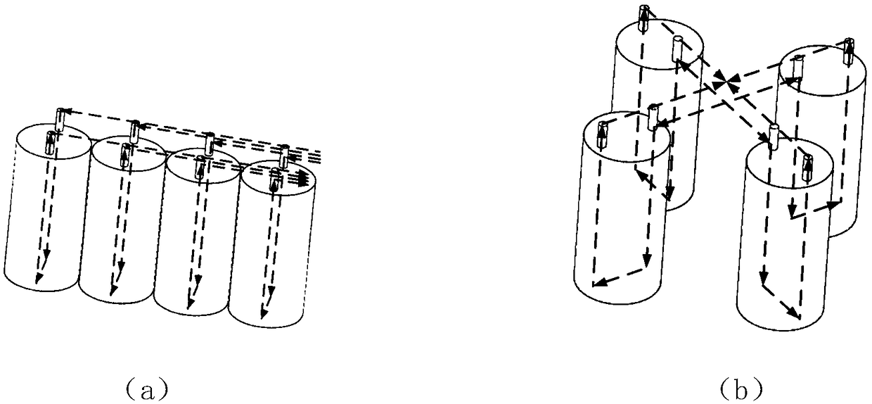
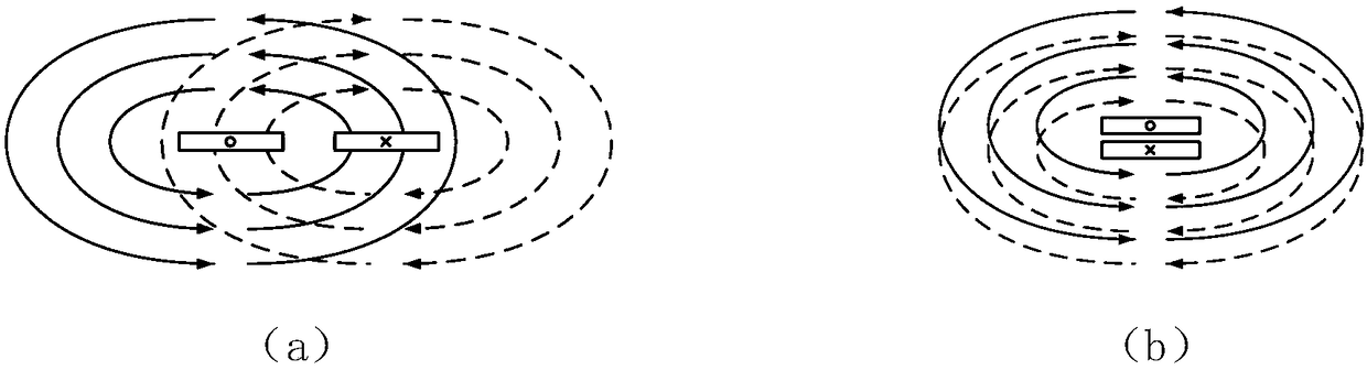
[0050] The purpose of the present invention is to provide a new type of DC busbar, which can effectively reduce the parasitic inductance of the DC busbar, thereby avoiding the excessive voltage overshoot of the drain and source during the turn-off process of the silicon carbide power MOSFET device, and further The damage rate of silicon carbide MOSFET devices is reduced.

[0051] In order to make the above objects, features and advantages of the present invent...


PUM


Abstract

The invention discloses a novel DC busbar. The DC busbar includes: absorbing capacitors, energy storage capacitors, positive poles, negative poles, and an insulating layer; the discharge positions of multiple energy storage capacitors are in a ring structure, and multiple energy storage capacitors are connected in parallel; the positive pole and One end of the energy storage capacitor is connected; the other end of the energy storage capacitor is connected to the negative electrode; the insulating layer is stacked on the positive electrode; the negative electrode is stacked on the insulating layer; The discharge position of the absorbing capacitor is also in a ring structure; the absorbing capacitor is located on the negative pole; the absorbing capacitor is used to reduce parasitic inductance; multiple absorbing capacitors are connected in parallel; the energy storage capacitor and the Snubber capacitors are connected in parallel. The use of the DC busbar provided by the present invention can effectively reduce the parasitic inductance in the power loop, thereby reducing the voltage and current overshoot of the silicon carbide power device during the switching process, reducing switching loss, and improving the service life of the silicon carbide power device.

Description

technical field [0001] The invention relates to the technical field of power electronics, in particular to a novel DC busbar. Background technique [0002] In recent years, silicon carbide power semiconductor devices have gradually attracted people's attention because of their good material properties such as higher critical breakdown field strength, better thermal conductivity, low on-state resistance, and high switching frequency. Bipolar transistors (Insulated Gate Bipolar Transistor, IGBT), devices, silicon carbide power semiconductor devices have shorter switching times, lower switching losses, and can achieve higher switching frequencies, so they are often used in high-frequency high-power density converters In order to reduce the size of its output filter, thereby reducing the size, weight and volume of the entire power electronic device. [0003] In high-frequency converter applications, the commonly used SiC power semiconductor devices are SiC Metal-Oxide-Semicondu...

Claims


Application Information

Patent Timeline
Patent Type & Authority Patents(China)
IPC IPC(8): H02M1/34
CPCH02M1/34H02M1/348Y02B70/10
Inventor 柯俊吉谢宗奎张希蔚徐鹏赵志斌崔翔
Owner NORTH CHINA ELECTRIC POWER UNIV (BAODING)
Why Eureka
Try Eureka