Single-layer gold nano-structure capable of realizing asymmetric transmission and preparation method thereof
An asymmetric transmission and gold nanostructure technology, which is applied in the field of single-layer gold nanostructure and its preparation, can solve the problems of complex three-dimensional structure, low asymmetric transmission effect, and slow etching, so as to improve preparation efficiency and save exposure The effect of simple time and structure
- Summary
- Abstract
- Description
- Claims
- Application Information
AI Technical Summary
Problems solved by technology
Method used
Image
Examples
Embodiment 1
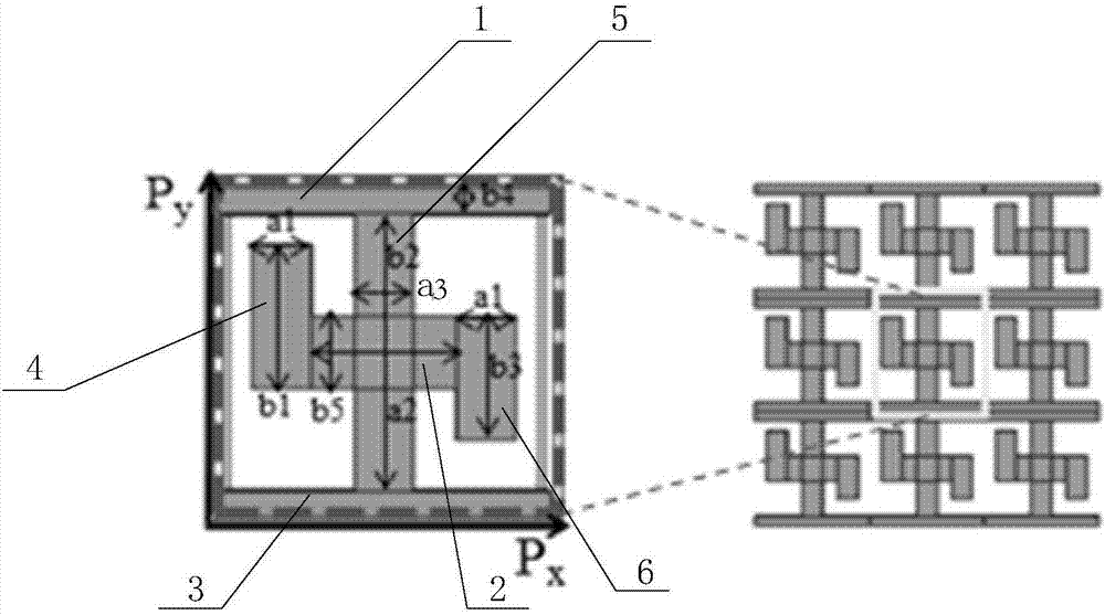
[0050] Such as figure 2 The single-layer gold nanostructure for asymmetric transmission shown in the right figure is composed of multiple identical structural units connected up and down, left and right. The structural diagram of each structural unit is shown in figure 2 As shown in the figure on the left, the structural unit is a single-layer structure with equal periodic side lengths, and all structural units are located on the same plane; the structural unit includes the first horizontal body 1, the second horizontal body 2 and the third horizontal body 3, The first horizontal body 1, the second horizontal body 2 and the third horizontal body 3 are parallel to each other, the distance between the second horizontal body 2, the first horizontal body 1 and the third horizontal body 3 is equal, and the first horizontal body 1, the second horizontal body The centers of the horizontal body 2 and the third horizontal body 3 are on the same straight line; the lengths of the secon...
Embodiment 2
[0070] Based on the parameters and steps of Example 1, after the single-layer gold nanostructure for realizing asymmetric transmission of the present invention is prepared, a calculation simulation test is performed by using the three-dimensional finite element method (FEM) calculation software COMSOL Multiphysics.
[0071] Such as figure 2 As shown, the parameters of the set structure are a1=57nm; a2=140nm; a3=57nm; b1=140nm; b2=270nm; b3=120nm; b4=25nm;
[0072] When preparing the structure of this embodiment, after using a pattern generator to set according to the above structure, the structure pattern is exposed with an electron beam, and the rest of the steps are the same as the preparation method in Example 1.
[0073] The transmission spectrum of the single-layer gold nanostructure that realizes asymmetric transmission prepared in this example is as follows Figure 4 shown, from Figure 4 It can be seen that at the resonance positions of 650nm and 1300nm, the convers...
Embodiment 3
[0081] In the single-layer gold nanostructure for realizing asymmetric transmission in this embodiment, only the width of the second horizontal body 2 is changed, and other parameters remain unchanged, which are the same as in Embodiment 2. In the structure of this embodiment, the width b5 of the second horizontal body 2 is 80 nm.
[0082] The transmission spectrum of the single-layer gold nanostructure that realizes asymmetric transmission prepared in this example is as follows Figure 8 As shown, the conversion rate of the asymmetric transmission of the monolayer gold nanostructure that realizes the asymmetric transmission of the present embodiment is as follows Figure 9 shown.
[0083] Will Figure 8 , Figure 9 with Example 2 Figure 4 , Figure 5 By comparison, it can be seen that after changing the parameters of b5, the resonance position of the transmission line is compared with that before the change, the resonance mode does not change, but the resonance position...
PUM
| Property | Measurement | Unit |
|---|---|---|
| width | aaaaa | aaaaa |
| length | aaaaa | aaaaa |
| width | aaaaa | aaaaa |
Abstract
Description
Claims
Application Information
 - R&D Engineer
- R&D Manager
- IP Professional
- Industry Leading Data Capabilities
- Powerful AI technology
- Patent DNA Extraction
Browse by: Latest US Patents, China's latest patents, Technical Efficacy Thesaurus, Application Domain, Technology Topic, Popular Technical Reports.
© 2024 PatSnap. All rights reserved.Legal|Privacy policy|Modern Slavery Act Transparency Statement|Sitemap|About US| Contact US: help@patsnap.com


