Thin film transistor and manufacturing method thereof, display panel and display device
A technology for thin film transistors and gates, applied in the fields of display panels and display devices, thin film transistors and their manufacturing methods, can solve the problems such as the ineffectiveness of products and the influence of the performance of thin film transistors, so as to reduce stress, improve quality, and avoid damage Effect
- Summary
- Abstract
- Description
- Claims
- Application Information
AI Technical Summary
Problems solved by technology
Method used
Image

Examples
Embodiment 1
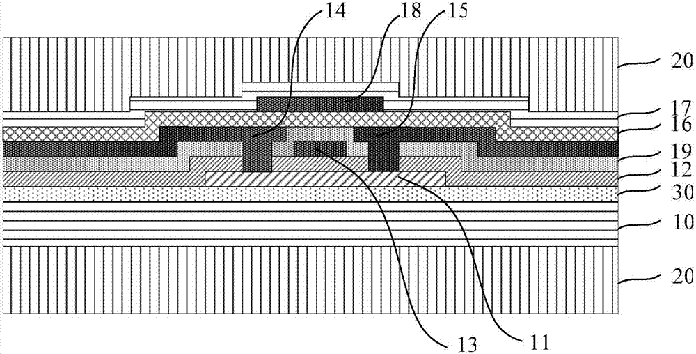
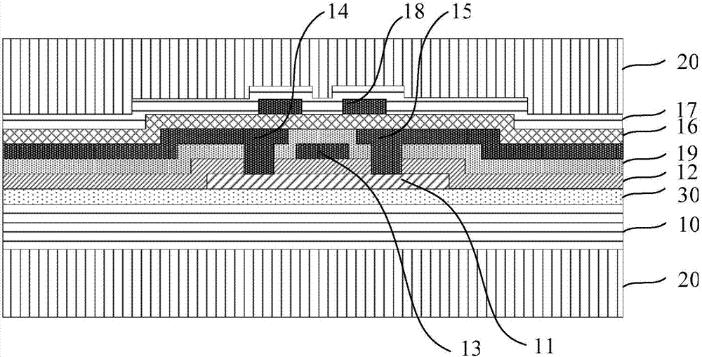
[0027] figure 1 A schematic structural diagram of a thin film transistor provided in Embodiment 1 of the present invention, as shown in figure 1 As shown, the thin film transistor proposed in this embodiment includes an active region 11, a gate insulating layer 12, a gate 13, a source 14, a drain 15, a passivation layer 16 and a flat surface formed sequentially on a flexible substrate 10. A protection layer 17 is formed between the passivation layer 16 and the planarization layer 17 , and the protection layer 18 is located directly above the active region 11 and the gate 13 .
[0028] from figure 1 It can be seen from the figure that the protection layer 18 is located directly above the active region 11 and the gate 13, and the protection layer 18 completely covers the gate 13 in a direction perpendicular to the gate 13. The material of the protective layer 18 is organic or metal, and can also be other materials known to those skilled in the art. The protective layer 18 has...
Embodiment 2
[0034] The present invention provides a method for preparing the thin film transistor described in Embodiment 1, comprising: sequentially forming an active region 11, a gate insulating layer 12, a gate 13, a source 14 and a drain 15 on a flexible substrate 10, and A passivation layer 17, a protective layer 18 is formed on the passivation layer 16, a planarization layer 17 is formed on the protective layer 18; the protective layer 18 is located between the active region 11 and the gate 13 Directly above. finally formed figure 1 or figure 2 structure shown.
[0035] The protective layer 18 has a protective effect on the semiconductor material in its vertical region, thereby reducing the stress on some materials of the thin film transistor during the bending process, avoiding possible damage to the semiconductor material during the bending process of the thin film transistor device, and thereby improving the reliability of the device. quality.
[0036] The protective layer 1...
Embodiment 3
[0038] This embodiment provides a display panel, which includes the thin film transistor described in the first embodiment.
[0039]The display panel of this embodiment has the thin film transistor in the first embodiment, so a protection layer is formed between the passivation layer and the planarization layer of the thin film transistor, and the protection layer is located between the active region and the gate. Directly above, it has a protective effect on the semiconductor material in its vertical region, thereby reducing the stress on some materials of the thin film transistor during the bending process, avoiding possible damage to the semiconductor material during the bending process of the thin film transistor device, and thus improving the quality of the device When the protective layer is made of a metal material, the protective layer covers the gap between the active region, the grid, the source and the drain in a direction perpendicular to the grid, because the mater...
PUM
 Abstract
Description
Claims
Application Information
 - R&D
- Intellectual Property
- Life Sciences
- Materials
- Tech Scout
- Unparalleled Data Quality
- Higher Quality Content
- 60% Fewer Hallucinations
Browse by: Latest US Patents, China's latest patents, Technical Efficacy Thesaurus, Application Domain, Technology Topic, Popular Technical Reports.
© 2025 PatSnap. All rights reserved.Legal|Privacy policy|Modern Slavery Act Transparency Statement|Sitemap|About US| Contact US: help@patsnap.com