Level switching circuit and method

A technology for converting circuits and levels, which is applied in logic circuits, eliminating voltage/current interference, logic circuit connection/interface layout, etc.

Active Publication Date: 2017-08-25
SHANGRUI MICROELECTRONICS SHANGHAI
View PDF5 Cites 6 Cited by
  • Summary
  • Abstract
  • Description
  • Claims
  • Application Information

AI Technical Summary

Problems solved by technology

[0004] However, during the switching process of the input level signal Sp, due to the simultaneous switching of the level signals, M1 and M3, M2 and M4, M5 and M7, M6 and M8 may all be turned on at the same time, so that the positive power supply VDD to the negative power supply VNEG A loop is generated between them, resulting in leakage; this will not only consume more dynamic current, but also cause more burrs on the edge of the output voltage signal, making it difficult to provide a high-quality control level for the subsequent circuit

Method used


Image

  • Level switching circuit and method
  • Level switching circuit and method
  • Level switching circuit and method

Examples


Embodiment Construction

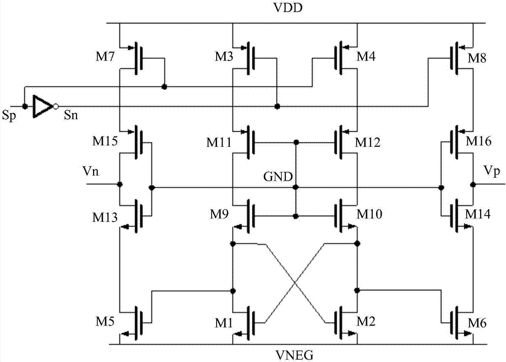
[0061] The level conversion circuit provided by the embodiment of the present invention is mainly used in the design of integrated circuits. By adjusting the timing of the level signal, it is avoided that the positive power supply VDD and the negative power supply VNEG are turned on simultaneously due to the simultaneous conduction of the PMOS transistor and the NMOS transistor. The leakage caused by the loop can significantly reduce the dynamic current and reduce the edge glitch of the output voltage signal.

[0062] The realization of the purpose of the present invention, functional characteristics and advantages will be further described in conjunction with the embodiments and with reference to the accompanying drawings. It should be understood that the specific embodiments described here are only used to explain the present invention, not to limit the present invention.

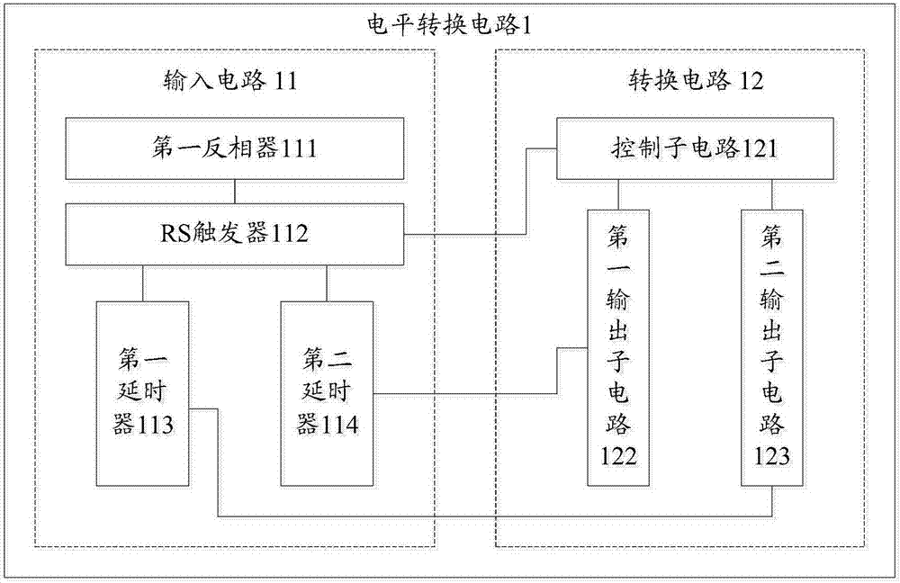
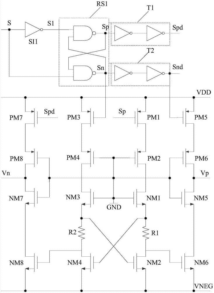
[0063] figure 2 It is a schematic block diagram of the first embodiment of the level conversion circ...


PUM


Abstract

The invention discloses a level switching circuit, which comprises an input circuit and a switching circuit, wherein the input circuit is used for carrying out inverse and delay operations on an input level signal to obtain a first level signal, a second level signal, a third level signal and a fourth level signal; a rising edge of the first level signal is first preset time easier than a falling edge of the second level signal, and a falling edge of the first level signal is second preset time later than a rising edge of the second level signal; the third level signal is obtained by delaying the first level signal for third preset time, and the fourth level signal is obtained by delaying the second level signal for fourth preset time; the first preset time is greater than the third preset time and the second preset time is greater than the fourth preset time; and the switching circuit is used for outputting a first voltage signal and a second voltage signal according to the level signals. The invention also discloses a level switching method.

Description

technical field [0001] The invention relates to the technical field of integrated circuits, in particular to a level conversion circuit and method. Background technique [0002] The level conversion circuit is widely used in various interface circuits and input and output units to realize the logic conversion of the level, figure 1 It is a schematic diagram of the circuit structure for level conversion in integrated circuit design. It is often used to convert the logic level from the ground level GND to the positive power supply VDD to the logic level from the negative power supply VNEG to the positive power supply VDD. For example, 0~ The voltage of 2.5V is converted into the voltage of -2.5~2.5V. refer to figure 1 As shown, the level conversion circuit includes 16 Metal-Oxide Semiconductor Field Effect Transistors (MOS-FET, Metal-Oxide Semiconductor Field Effect Transistor), represented by M1~M16 respectively; wherein, M1~M4 are used to MOS tubes for level conversion; M...

Claims


Application Information

Patent Timeline
IPC IPC(8): H03K19/0185H03K19/003
CPCH03K19/00361H03K19/018507
Inventor 马军王鑫奕江涛
Owner SHANGRUI MICROELECTRONICS SHANGHAI
Why Eureka
Try Eureka