A chip double-sided vertical packaging structure and packaging method

A packaging method and packaging structure technology, applied in the direction of semiconductor/solid-state device parts, semiconductor devices, electrical components, etc., can solve the problems of uneven upper and lower contact surfaces, large stress distribution of packaged products, and low online precision, etc., to achieve a good surface Flatness, adjustable packaging stress, compact size

Active Publication Date: 2019-09-03
CHINA RESOURCES MICROELECTRONICS (CHONGQING) CO LTD
View PDF4 Cites 0 Cited by
  • Summary
  • Abstract
  • Description
  • Claims
  • Application Information

AI Technical Summary

Problems solved by technology

[0003] Traditional common chip mainstream packaging forms are roughly divided into: lead frame type, such as DIP (Dual In-line Package, dual in-line package), SOP (Small Outline Package, small size package), QFN (QuadFlatNo-lead Package, square Flat leadless package) and QFP (Plastic Quad Flat Package, square flat package), etc.; ball grid array type, such as: BGA (Ball Grid Array Package, ball grid array package), FC-BGA (FlipChip BGA, flip chip technology ball grid array package) and μBGA, etc., these packaging methods need to connect the poles of the chip to the external pins and frames through leads, or directly connect and bond with the pins and frames, so that the volume of the final package is often It is several times larger than the chip itself, especially in the vertical direction, the thickness is relatively large, and there is a large stress distribution inside the packaged product, and at the same time, it is easy to produce relatively uneven upper and lower contact surfaces, resulting in low online accuracy. Problems limit the application on ultra-thin electronic systems (such as electronic smart wearable devices, etc.), which is not expected by those skilled in the art

Method used


Image

  • A chip double-sided vertical packaging structure and packaging method
  • A chip double-sided vertical packaging structure and packaging method
  • A chip double-sided vertical packaging structure and packaging method

Examples


Embodiment 1

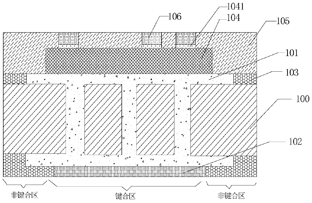
[0052] Such as figure 1As shown, this embodiment relates to a chip 104 double-sided vertical package structure, the package structure includes a PCB board 100, a conductive material layer 101, a first solder layer 102, a PCB solder resist layer 103, and a plurality of pads 1041 chip 104 are provided. , the plastic sealing layer 105 and the second solder layer 106; specifically, the above-mentioned PCB board 100 includes the PCB board 100 of the bonding area and the non-bonding area, and the PCB board 100 of the bonding area is provided with several conductive structures throughout; The material layer 101 includes a first conductive layer covering the upper surface of the PCB board 100 in the bonding area and a second conductive layer covering the lower surface of the PCB board 100 in the bonding area, and the first conductive layer and the second conductive layer pass through the above-mentioned several conductive layers. Structural electrical connection; the first solder laye...

Embodiment 2

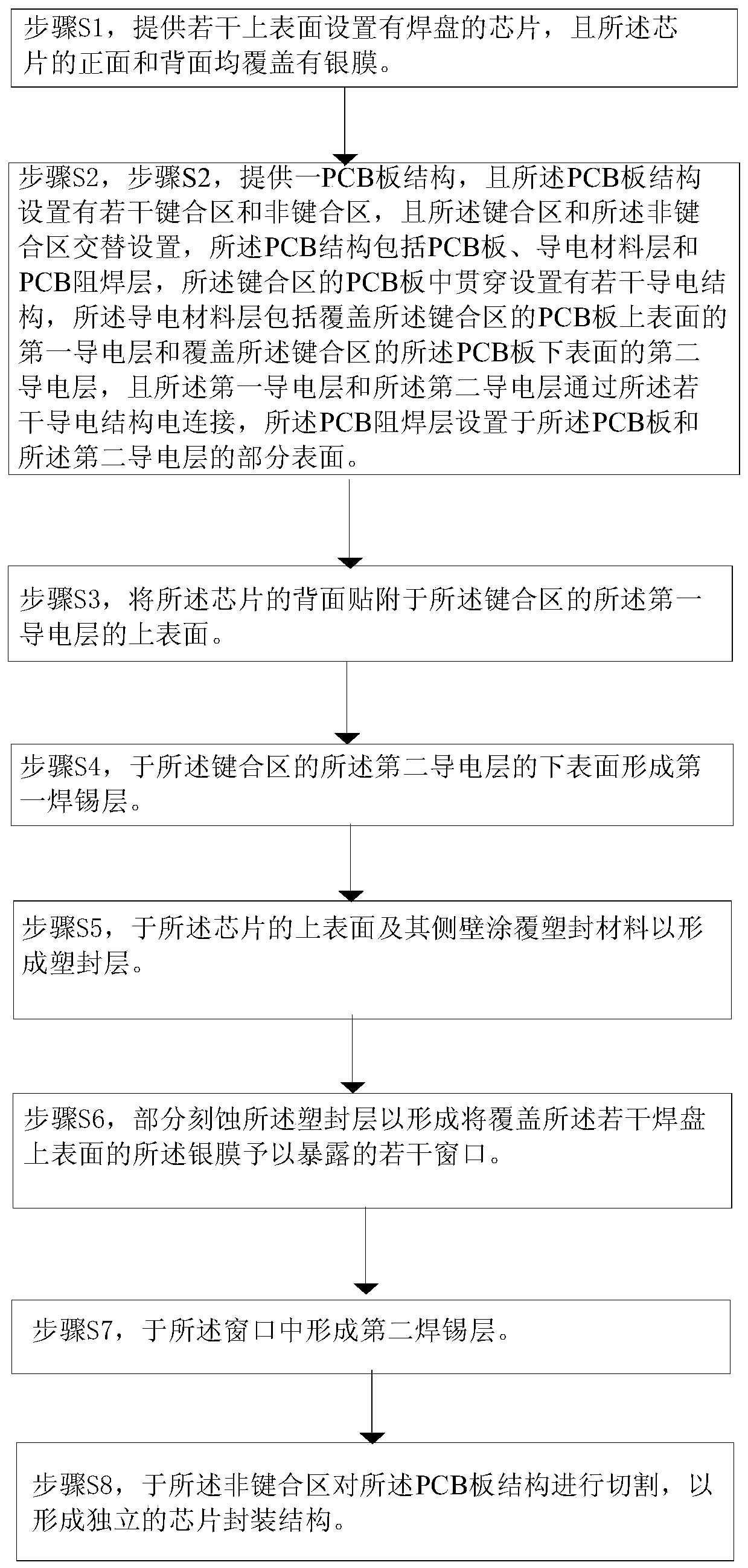
[0058] Such as figure 2 As shown, the present invention relates to a double-sided vertical packaging method for a chip 200. Specifically, the packaging method includes the following steps:

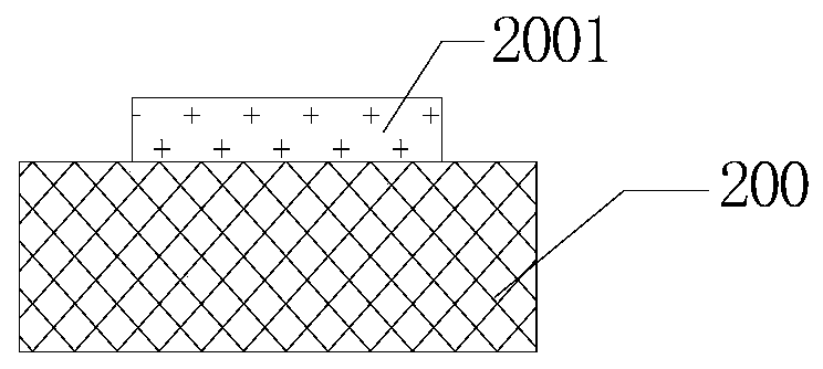
[0059] Step S1, provide several chips 200 with pads 2001 on the upper surface, and the front and back of the several chips 200 are covered with silver film (not shown in the figure), as image 3 structure shown.

[0060] In a preferred embodiment of the present invention, the chip 200 has a thickness of 30-500 μm (eg 30 μm, 200 μm, 265 μm or 500 μm).

[0061] In a preferred embodiment of the present invention, the thickness of the silver film is 1-9 μm (eg 1 μm, 3 μm, 5 μm or 9 μm, etc.).

[0062] In a preferred embodiment of the present invention, the above step S1 includes:

[0063] Step S11 , providing a wafer including a plurality of chips 200 , and each chip 200 is provided with a plurality of bonding pads 2001 (which may be one or more bonding pads 2001 ) on the upper surface.

...


PUM


Abstract

The invention relates to the technical field of semiconductor manufacturing, and especially relates to a chip double-side vertical packaging structure and a packaging method. After a PCB structure with a conductive material layer is prepared, a chip is bonded onto the conductive material in a bonding area of the PCB structure. After a first solder layer is formed on the back of the PCB structure, the chip is plastically packaged with a plastic package material, the plastic package material is windowed, and a second solder layer is formed in the window. Therefore, ultra-thin and high-performance vertical chip package is realized under the condition of minimum size. The chip double-side vertical packaging structure has the advantages of small size and high reliability.

Description

technical field [0001] The invention relates to the technical field of semiconductor manufacturing, in particular to a chip double-sided vertical packaging structure and packaging method. Background technique [0002] At present, chip packaging technology is constantly pursuing the development of thinness, miniaturization, portability, high reliability, low power consumption and low cost. [0003] Traditional common chip mainstream packaging forms are roughly divided into: lead frame type, such as DIP (Dual In-line Package, dual in-line package), SOP (Small Outline Package, small size package), QFN (QuadFlatNo-lead Package, square Flat leadless package) and QFP (Plastic Quad Flat Package, square flat package), etc.; ball grid array type, such as: BGA (Ball Grid Array Package, ball grid array package), FC-BGA (FlipChip BGA, flip chip technology ball grid array package) and μBGA, etc., these packaging methods need to connect the poles of the chip to the external pins and fram...

Claims


Application Information

Patent Timeline
Patent Type & Authority Patents(China)
IPC IPC(8): H01L23/31H01L23/498H01L23/00H01L21/48H01L21/56
Inventor 张小辛
Owner CHINA RESOURCES MICROELECTRONICS (CHONGQING) CO LTD
Why Eureka
Try Eureka