A method of manufacturing a light-emitting diode epitaxial wafer

A technology for light-emitting diodes and a manufacturing method, which is applied to semiconductor devices, electrical components, circuits, etc., can solve the problems of reduction of production cycle and cost, inability to increase the growth rate of high-temperature buffer layer, etc., and achieve the effect of improving crystal quality and realizing growth cycle.

Active Publication Date: 2019-03-08
HC SEMITEK ZHEJIANG CO LTD
View PDF5 Cites 0 Cited by
  • Summary
  • Abstract
  • Description
  • Claims
  • Application Information

AI Technical Summary

Problems solved by technology

[0006] In order to solve the problem that the prior art cannot increase the growth rate of the high-temperature buffer layer to reduce the production cycle and cost, an embodiment of the present invention provides a method for manufacturing a light-emitting diode epitaxial wafer

Method used


Image

  • A method of manufacturing a light-emitting diode epitaxial wafer
  • A method of manufacturing a light-emitting diode epitaxial wafer
  • A method of manufacturing a light-emitting diode epitaxial wafer

Examples


Embodiment

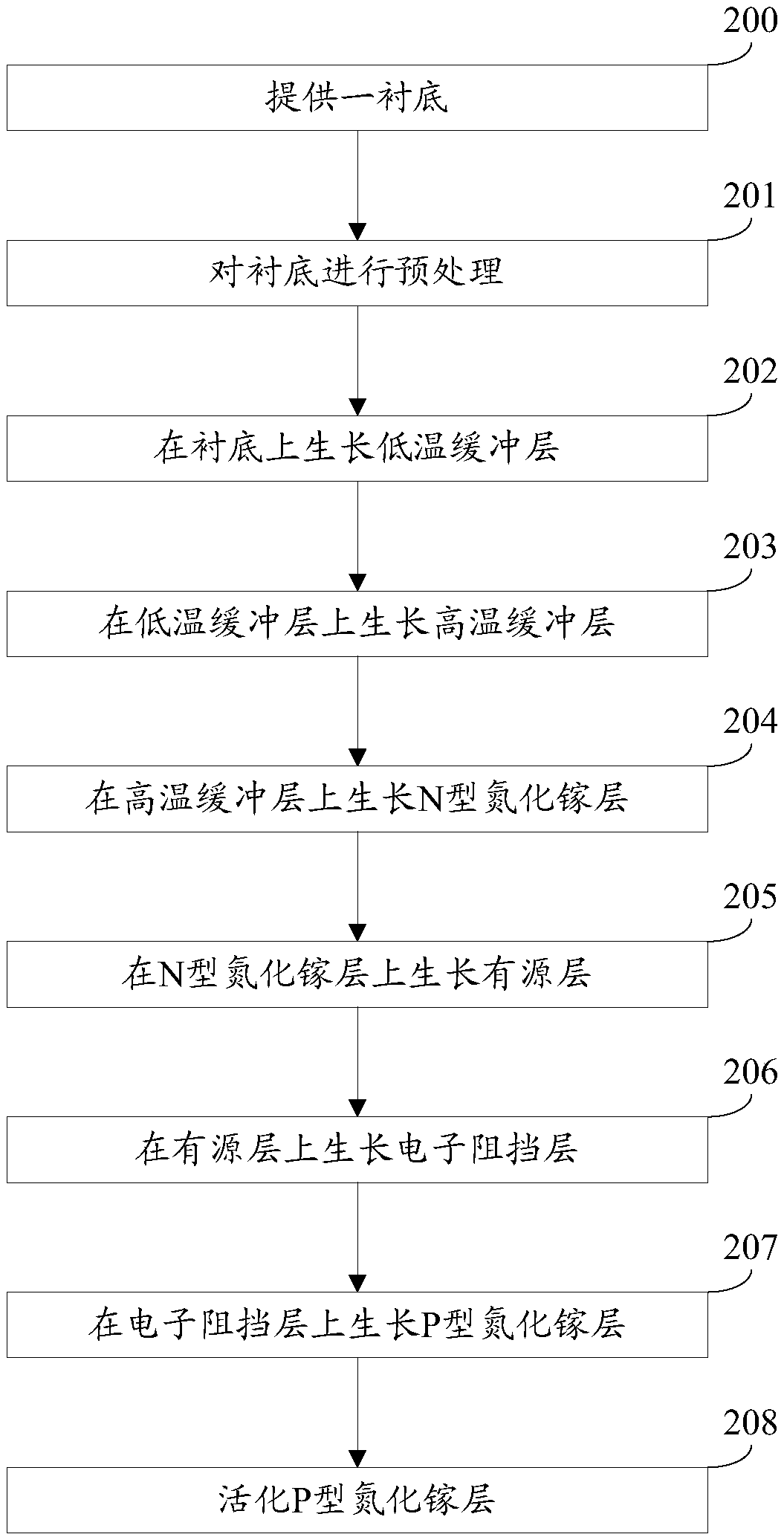
[0028] An embodiment of the present invention provides a method for manufacturing a light-emitting diode epitaxial wafer. In this embodiment, Veeco K465i or C4 metal organic compound chemical vapor deposition (English: Metal Organic Chemical VaporDeposition, referred to as: MOCVD) equipment is used to realize the LED epitaxial wafer. manufacturing. Using high-purity hydrogen (H 2 ) or high-purity nitrogen (N 2 ) or high purity H 2 and high purity N 2 The mixed gas as the carrier gas, high-purity NH 3 As nitrogen source, trimethylgallium (TMGa) and triethylgallium (TEGa) as gallium source, trimethylindium (TMIn) as indium source, trimethylaluminum (TMAl) as aluminum source, silane (SiH4) as N-type dopant, magnesium dicene (CP 2 Mg) as a P-type dopant. The pressure of the reaction chamber is controlled at 100-600 torr.

[0029] Specifically, see figure 1 , the growth method includes:

[0030] Step 200: Provide a substrate.

[0031] In this embodiment, the substrate is ...


PUM


Abstract

The invention discloses a manufacturing method for a light emitting diode epitaxial wafer, which belongs to the technical field of semiconductors. The method comprises the steps that a substrate is provided; a low temperature buffer layer, a high temperature buffer layer, an N type gallium nitride layer, an active layer, an electron blocking layer and a P type gallium nitride layer successively grow on the substrate; the high temperature buffer layer comprises (n+1) gallium nitride layers and n aluminum gallium nitride layers, wherein n is a positive integer and (n+1) gallium nitride layers and n aluminum gallium nitride layers are alternately stacked; the growth temperature of (n+1) gallium nitride layers increases layer by layer along the growth direction of the light emitting diode epitaxial wafer; the growth rate of (n+1) gallium nitride layers accelerates layer by layer along the growth direction of the light emitting diode epitaxial wafer; and the aluminum component content in n aluminum gallium nitride layers increases layer by layer along the growth direction of the light emitting diode epitaxial wafer. According to the invention, the improvement of the growth temperature of the gallium nitride layers and the aluminum component content in the aluminum gallium nitride layers compensates for defects produced by the improvement of the growth rate; the growth cycle is reduced; and the production cost is reduced.

Description

technical field [0001] The invention relates to the technical field of semiconductors, in particular to a method for manufacturing a light-emitting diode epitaxial wafer. Background technique [0002] A light-emitting diode (English: Light Emitting Diode, referred to as: LED) is a semiconductor electronic component that can emit light. As an efficient, environmentally friendly, and green new solid-state lighting source, LEDs are rapidly and widely used in traffic lights, automotive interior and exterior lights, urban landscape lighting, and mobile phone backlights. [0003] The epitaxial wafer of the existing LED includes a substrate, and a low-temperature buffer layer, a high-temperature buffer layer, an N-type gallium nitride layer, an active layer, an electron blocking layer, and a P-type gallium nitride layer sequentially stacked on the substrate. Wherein, both the low-temperature buffer layer and the high-temperature buffer layer are gallium nitride layers grown under ...

Claims


Application Information

Patent Timeline
Patent Type & Authority Patents(China)
IPC IPC(8): H01L33/00H01L33/12H01L33/32
CPCH01L33/0075H01L33/12H01L33/325
Inventor 姚振从颖胡加辉
Owner HC SEMITEK ZHEJIANG CO LTD
Why Eureka
Try Eureka