Capacitance compensation and design method of gold wire bonding in a three-dimensional package circuit

A technology of capacitance compensation and three-dimensional packaging, which is applied to circuits, including printed capacitors, electrical components, etc., can solve the problems of occupying design space and limited improvement of microwave transmission performance, and achieve reduced area, compact structure, and low return loss. increased effect

Active Publication Date: 2020-05-19
CHINA ELECTRONIC TECH GRP CORP NO 38 RES INST
View PDF1 Cites 0 Cited by
  • Summary
  • Abstract
  • Description
  • Claims
  • Application Information

AI Technical Summary

Problems solved by technology

However, these capacitive compensation methods for gold wire bonding generally have a problem, that is, the capacitive compensation structure is only designed on the surface transmission line, which greatly occupies the design space
In miniaturized, multi-channel packaged circuits, obviously there is not so much area for impedance matching design of gold wire bonding
In addition, these methods of capacitive compensation design only by increasing the size of the pad have limited improvement in microwave transmission performance

Method used


Image

  • Capacitance compensation and design method of gold wire bonding in a three-dimensional package circuit
  • Capacitance compensation and design method of gold wire bonding in a three-dimensional package circuit
  • Capacitance compensation and design method of gold wire bonding in a three-dimensional package circuit

Examples


Embodiment Construction

[0031] The embodiments of the present invention are described in detail below. This embodiment is implemented on the premise of the technical solution of the present invention, and detailed implementation methods and specific operating procedures are provided, but the protection scope of the present invention is not limited to the following implementation example.

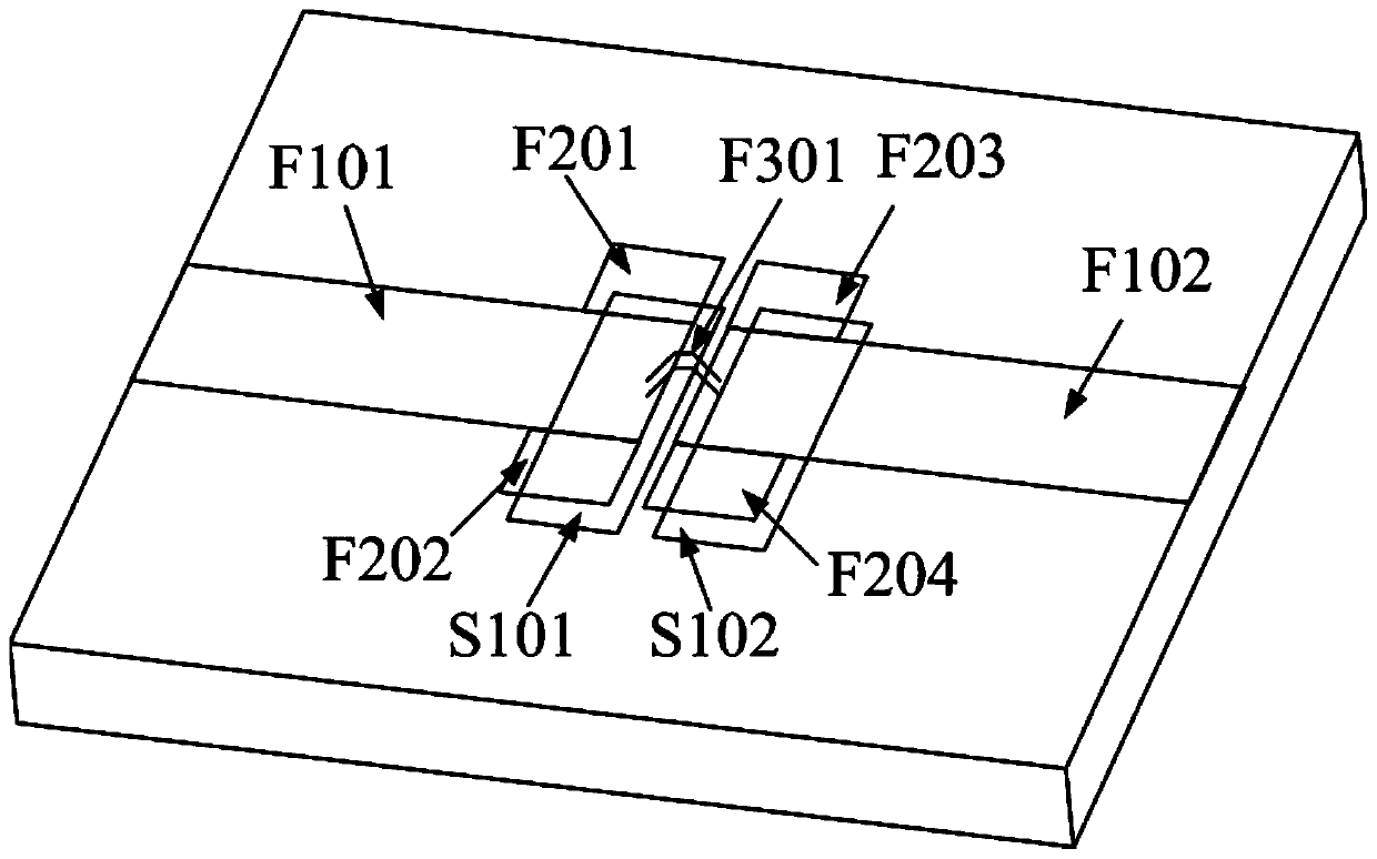
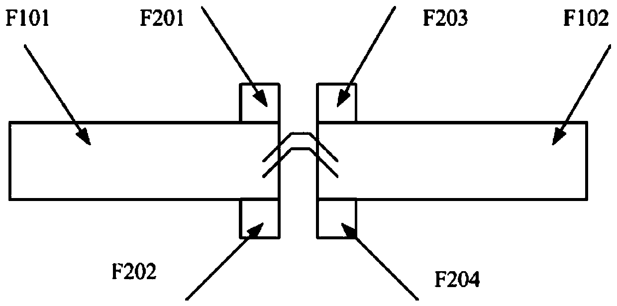
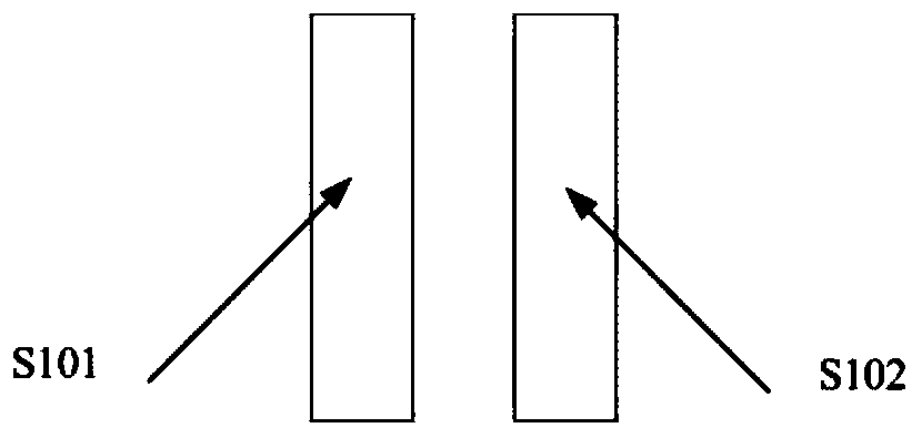
[0032] Such as figure 1 As shown, it is a three-dimensional diagram of the multilayer circuit gold wire bonding capacitance compensation design method according to the present invention, and the gold wire bonding F301 is connected between two 50-ohm first transmission lines F101 and second transmission lines F102. Wherein, the 50-ohm first transmission line F101 can be an input port or an output port, and correspondingly, the 50-ohm second transmission line F102 is an output port or an input port, and the two 50-ohm first transmission lines F101 and the second The transmission lines F102 are all in the form of 50 ...


PUM

PropertyMeasurementUnit
thicknessaaaaaaaaaa
dielectric lossaaaaaaaaaa

Abstract

The invention discloses Gold wire bonding capacitance compensation in a three-dimensional encapsulated circuit. The invention involves a microwave multilayer circuit dielectric substrate. A capacitance compensation structure is arranged on a first layer transmission wire on the surface of the microwave multilayer circuit dielectric substrate. A capacitance compensation structure is arranged on a middle layer transmission wire in the vertical direction of the microwave multilayer circuit dielectric substrate. The transmission lines are in interconnection through gold wire bond wires. According to the invention, a problem of impedance matching of gold wire bonding in the three-dimensional encapsulated circuit is solved effectively. Space of the multilayer circuit is utilized fully for design of the capacitance compensation structure for parasitic inductance effect of gold wire bonding, especially the capacitance compensation structure added in the vertical direction. Compared with a prior art, area required for capacitance compensation merely on the surface layer transmission wire can be reduced. By adopting the structure provided by the invention, microwave transmission characteristics between transmission wires and chips and between transmission wires and transmission wires in a multi-chip circuit can be improved.

Description

technical field [0001] The invention relates to the technical field of microwave and millimeter wave packaged circuits, in particular to a capacitance compensation for gold wire bonding in a three-dimensional packaged circuit and a design method thereof. Background technique [0002] In the fields of radar, electronic countermeasures and communications, electronic systems are gradually developing towards high density, high speed, high reliability, high performance and low cost. As a representative of hybrid circuit integration technology, multi-chip circuits can design bare chips and various components into microwave integrated circuits that meet the needs in three-dimensional, multi-layer dielectric substrates and using micro-assembly and interconnection technology. [0003] In microwave multi-chip circuit technology, gold wire bonding technology is often used to realize the interconnection between microstrip transmission lines, monolithic microwave integrated circuits and ...

Claims


Application Information

Patent Timeline
Patent Type & Authority Patents(China)
IPC IPC(8): H01L23/66H01P5/02H05K1/16
CPCH01L23/66H01P5/02H05K1/162
Inventor 朱浩然倪涛戴跃飞
Owner CHINA ELECTRONIC TECH GRP CORP NO 38 RES INST
Why Eureka
Try Eureka