
TFT substrate, test method thereof and method for eliminating shutdown residual image

A substrate and test circuit technology, applied in nonlinear optics, instruments, optics, etc., can solve problems such as inaccurate positioning of array substrates, defective repairs, poor transmission of gate scanning signals, etc., so as to improve the detection rate of defects and eliminate shutdown Afterimage, display quality improvement effect

Inactive Publication Date: 2017-08-04
SHENZHEN CHINA STAR OPTOELECTRONICS SEMICON DISPLAY TECH CO LTD
View PDF4 Cites 13 Cited by
  • Summary
  • Abstract
  • Description
  • Claims
  • Application Information

AI Technical Summary

Problems solved by technology

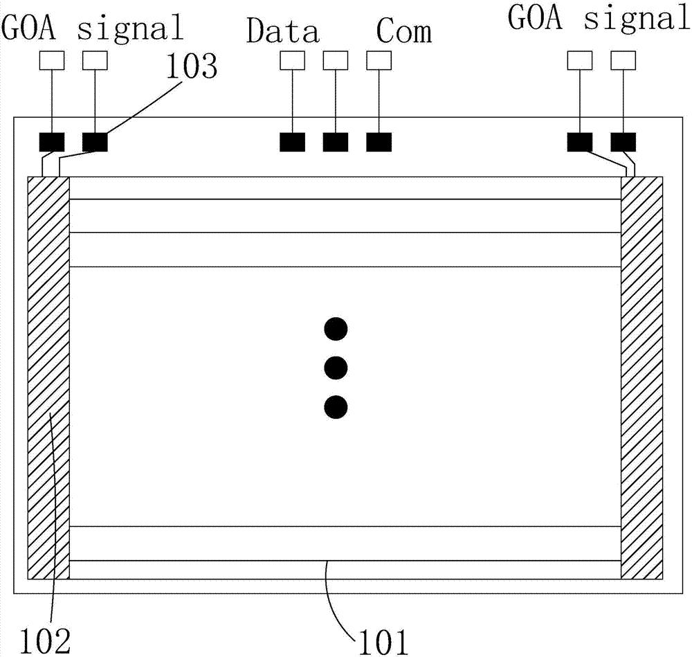
[0008] However, for the TFT substrate of GOA technology, the gate scanning signal needs to be generated by the GOA circuit 102 before being transmitted to the scanning line 101 in the display area. Poor grid scanning signal transmission (that is, defects in the horizontal direction), it is difficult to judge whether the scanning line 101 in the display area is defective or the GOA circuit 102 is defective, which leads to the inability to accurately locate the defective position of the array substrate for targeted defects repair

Method used


Image

  • TFT substrate, test method thereof and method for eliminating shutdown residual image
  • TFT substrate, test method thereof and method for eliminating shutdown residual image
  • TFT substrate, test method thereof and method for eliminating shutdown residual image

Examples


Embodiment Construction

[0049] In order to further illustrate the technical means adopted by the present invention and its effects, the following describes in detail in conjunction with preferred embodiments of the present invention and accompanying drawings.

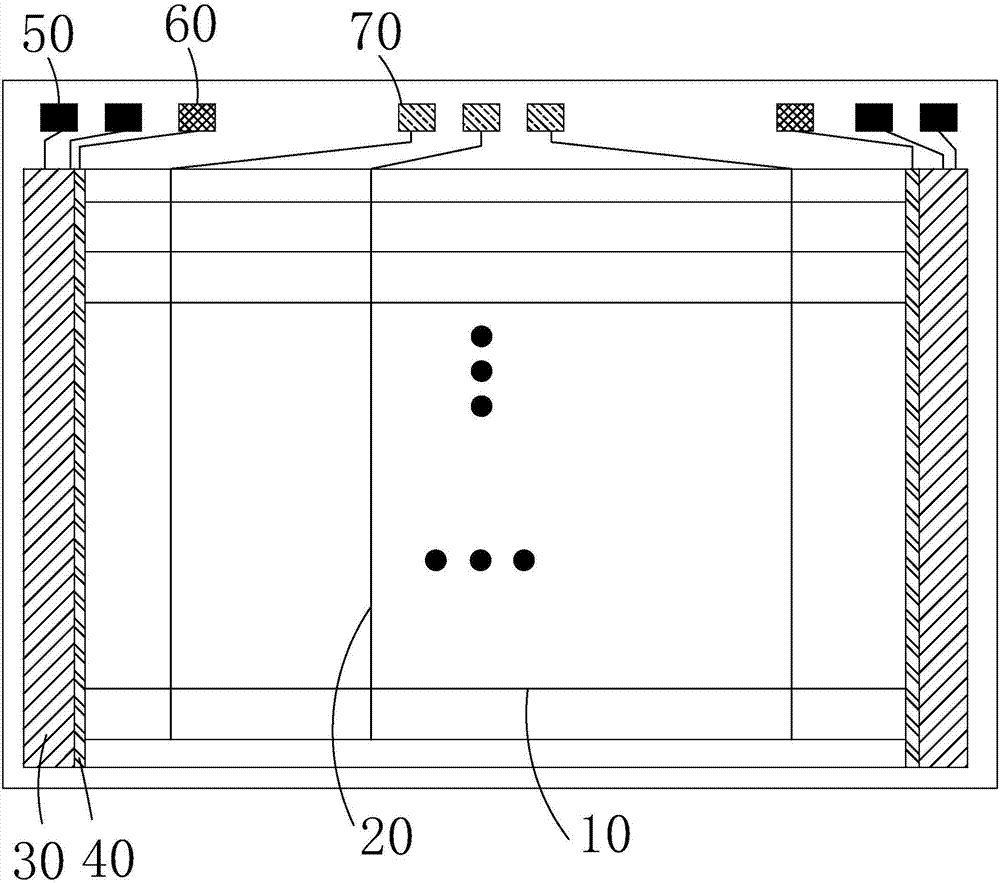
[0050] see image 3 or Figure 6 . The present invention provides a TFT substrate, comprising: a plurality of horizontal scan lines 10 arranged in parallel and spaced apart, a plurality of vertical data lines 20 arranged in parallel and spaced apart, and a GOA circuit electrically connected to the plurality of scan lines 10 30 and the in-plane test circuit 40, a plurality of GOA signal input points 50 electrically connected to the GOA circuit 30, at least one in-plane test signal input point 60 electrically connected to the in-plane test circuit 40, and all The plurality of data lines 20 correspond to the plurality of data signal input points 70 electrically connected one by one;

[0051] see Figure 4 , Figure 5 , Figure 7 ,or Figure...


PUM


Abstract

The invention provides a TFT substrate, a test method thereof and a method for eliminating a shutdown residual image. The TFT substrate is provided with an in-plane test circuit; the in-plane test circuit comprises a plurality of switch modules corresponding to a plurality of GOA units one to one and at least one switch control cabling line, each switch module comprises a control end, an input end and an output end, the control end and the input end are electrically connected with one switch control cabling line, the output end is electrically connected with scanning signal output ends of the GOA units corresponding to the switch control modules, each switch control cabling line is electrically connected with an in-plane test signal output point, an in-plane test signal is input to a scanning line through the switch control cabling lines and the switch modules so that fault detection can be conducted on the scanning line independently, and when a liquid crystal display device shuts down, a power discharge signal is input to the scanning line through the switch control cabling lines and the switch modules so that the shutdown residual image of the liquid crystal display device can be eliminated.

Description

technical field [0001] The invention relates to the field of display technology, in particular to a TFT substrate, a testing method thereof, and a method for eliminating residual images after shutdown. Background technique [0002] A Liquid Crystal Display (LCD) has many advantages such as a thin body, power saving, and no radiation, and has been widely used. Such as: LCD TV, mobile phone, personal digital assistant (PDA), digital camera, computer screen or notebook computer screen, etc., occupy a dominant position in the field of flat panel display. [0003] Most of the liquid crystal displays currently on the market are backlight liquid crystal displays, which include a liquid crystal display panel and a backlight module (Backlight Module). The working principle of the liquid crystal display panel is to pour liquid crystal molecules between the thin film transistor array substrate (ThinFilm Transistor Array Substrate, TFT Array Substrate) and the color filter substrate (C...

Claims


Application Information

Patent Timeline
IPC IPC(8): G02F1/1362G02F1/1345G09G3/00
CPCG02F1/13454G02F1/1362G02F1/136286G09G3/006G02F1/136254
Inventor 曾勉
Owner SHENZHEN CHINA STAR OPTOELECTRONICS SEMICON DISPLAY TECH CO LTD
Learn More