Deep ultraviolet LED epitaxial structure and fabrication method thereof

An epitaxial structure and deep ultraviolet technology, which is applied in the field of ultraviolet LEDs, can solve the difficulties in the production of high-quality P-type AlGaN, restrict the development of AlGaN deep ultraviolet LEDs, etc., achieve high luminous efficiency and ensure the effect of crystal quality

Pending Publication Date: 2017-07-25
ZEARAY WUHAN OPTOELECTRONICS TECH CO LTD
View PDF6 Cites 4 Cited by
  • Summary
  • Abstract
  • Description
  • Claims
  • Application Information

AI Technical Summary

Problems solved by technology

The band with the best bactericidal effect is around 265nm, and LEDs with a peak wavelength shorter than 270nm have higher requirements for Al components in AlGaN, and AlGaN materials with higher crystal quality and high Al components generally have larger defects and dislocation densities , high-quality P-type AlGaN is difficult to manufacture, these problems seriously restrict the development of AlGaN deep ultraviolet LED

Method used


Image

  • Deep ultraviolet LED epitaxial structure and fabrication method thereof
  • Deep ultraviolet LED epitaxial structure and fabrication method thereof
  • Deep ultraviolet LED epitaxial structure and fabrication method thereof

Examples


Embodiment Construction

[0021] The present invention will be further described in detail below in conjunction with the accompanying drawings and specific embodiments to facilitate a clear understanding of the present invention, but they do not limit the present invention.

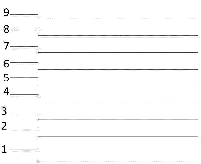
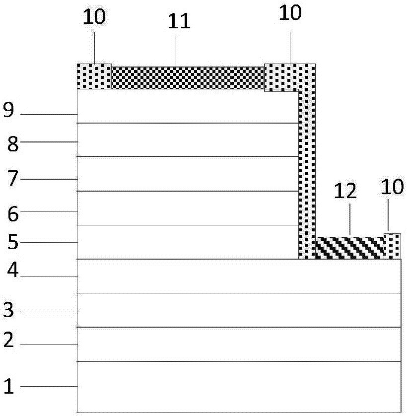
[0022] Such as figure 1 As shown, the epitaxial structure of the present invention is sequentially grown on the substrate material based on MOCVD, specifically:

[0023] The nucleation layer 2 is grown on a transparent substrate with a growth temperature of 950° C. and a growth pressure of 50 mbar; the nucleation layer 2 is made of GaN, AlN or AlGaN with a thickness of 10 nm-50 nm, and the thickness of this embodiment is 15 nm.

[0024] The substrate can be sapphire, AlN, GaN, etc.

[0025]The buffer layer 3 is grown on the nucleation layer, the growth temperature is 1200°C, and the growth pressure is 100mbar; the buffer layer 3 is unintentionally doped u-type AlGaN, the Al composition is 0.2-0.6, and the thickness is 1um-5um. T...


PUM

PropertyMeasurementUnit
Thicknessaaaaaaaaaa
Total thicknessaaaaaaaaaa

Abstract

The invention discloses a deep ultraviolet LED epitaxial structure and a fabrication method thereof. The deep ultraviolet LED epitaxial structure comprises a substrate, wherein a nucleating layer is grown on the substrate, a buffer layer is grown on the nucleating layer, an n-type AlGaN layer, a periodic structure AlGa<1-a>N / GaN current extension layer, a periodic structure AlGa<1-b>N / Al<c>Ga<1-c>N light-emitting layer, a periodic structure AlN / Al<d>Ga<1-d>N barrier layer, a periodic structure Al<e>Ga<1-e>N / GaN barrier layer and a p-type GaN layer are sequentially grown on the buffer layer, a Al<e>Ga<1-e>N layer in a Al<e>Ga<1-e>N / GaN barrier layer 8 is a unintentional doping layer, and a GaN layer is a Mg-doped layer. The periodic structure Al<e>Ga<1-e>N / GaN barrier layer is employed, Al<e>Ga<1-e>N is the unintentional doping layer, the GaN layer is the Mg-doped layer, holes are successfully introduced to the light-emitting layer by a memory effect of Mg and hole tunneling, electrons can be limited in the light-emitting layer by the barrier layer, the crystal quality of the barrier layer is also ensured, and the light-emitting efficiency is higher.

Description

technical field [0001] The invention belongs to the technical field of semiconductor devices, and in particular relates to a deep ultraviolet LED epitaxial structure and a preparation method thereof, in particular to an ultraviolet LED with an emission wavelength of about 265nm. Background technique [0002] The light wave with a wavelength between 100nm and 280nm belongs to deep ultraviolet light. The deep ultraviolet light source in this band has great application value in the fields of special lighting, sterilization, medical treatment, printing, biochemical detection, high-density information storage and secure communication. [0003] The forbidden band width of GaN is 3.4eV, and the forbidden band width of AlN is 6.2eV. Theoretically, the AlGaN material formed by GaN doped with Al can be made into an ultraviolet LED with a light emitting wavelength of 200nm to 365nm. The band with the best bactericidal effect is around 265nm, and LEDs with a peak wavelength shorter than...

Claims


Application Information

Patent Timeline
IPC IPC(8): H01L33/00H01L33/02H01L33/12H01L33/14H01L33/32
CPCH01L33/00H01L33/02H01L33/12H01L33/14H01L33/32
Inventor 孙卿汤磊罗邵军杨福华
Owner ZEARAY WUHAN OPTOELECTRONICS TECH CO LTD
Why Eureka
Try Eureka