A general test system and test method for radiation effects

A general-purpose test and radiation effect technology, applied in the field of radiation effect research, can solve the problems of high price of semiconductor professional test platform, difficulty in improving accuracy and clock speed, difficulty in meeting portability requirements, etc., and achieve convenient timing monitoring and high-precision timing monitoring , Simplify the effect of data analysis and processing

Active Publication Date: 2019-12-06
XIANGTAN UNIV +1
View PDF12 Cites 0 Cited by
  • Summary
  • Abstract
  • Description
  • Claims
  • Application Information

AI Technical Summary

Problems solved by technology

[0009] 1. Insufficient versatility, the existing test system is highly targeted, causing researchers to repeatedly face the problem of test system development
[0010] 2. It is difficult to improve the accuracy and clock speed of digital circuit test systems developed by researchers themselves
[0011] 3. The semiconductor professional test platform used in analog or digital-analog hybrid test is expensive and difficult to meet the portability requirements

Method used


Image

  • A general test system and test method for radiation effects
  • A general test system and test method for radiation effects
  • A general test system and test method for radiation effects

Examples


example 1

[0130] Example 1: DAC7621 static parameter total dose effect test

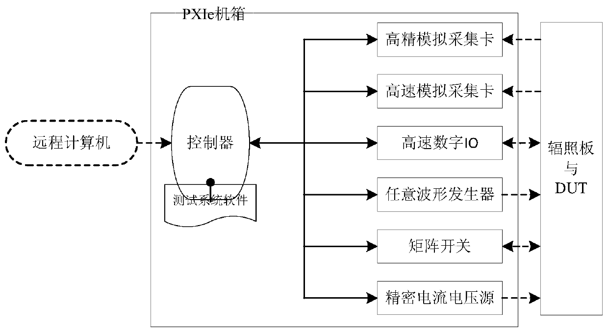
[0131] Test objective: Measure the transfer characteristic curve of the DAC and obtain parameters such as offset error Vos, gain error Eg, differential nonlinearity DNL, ​​integral nonlinearity INL, and full-scale output FSR through calculation and analysis. Test process hardware interconnection such as Figure 4 Shown:

[0132] Test method: DAC static parameter test is completed by testing transfer characteristic curve. The transfer characteristic curve is obtained by measuring the analog output corresponding to part or all of the digital code value input. The test process is as follows: Figure 5 shown.

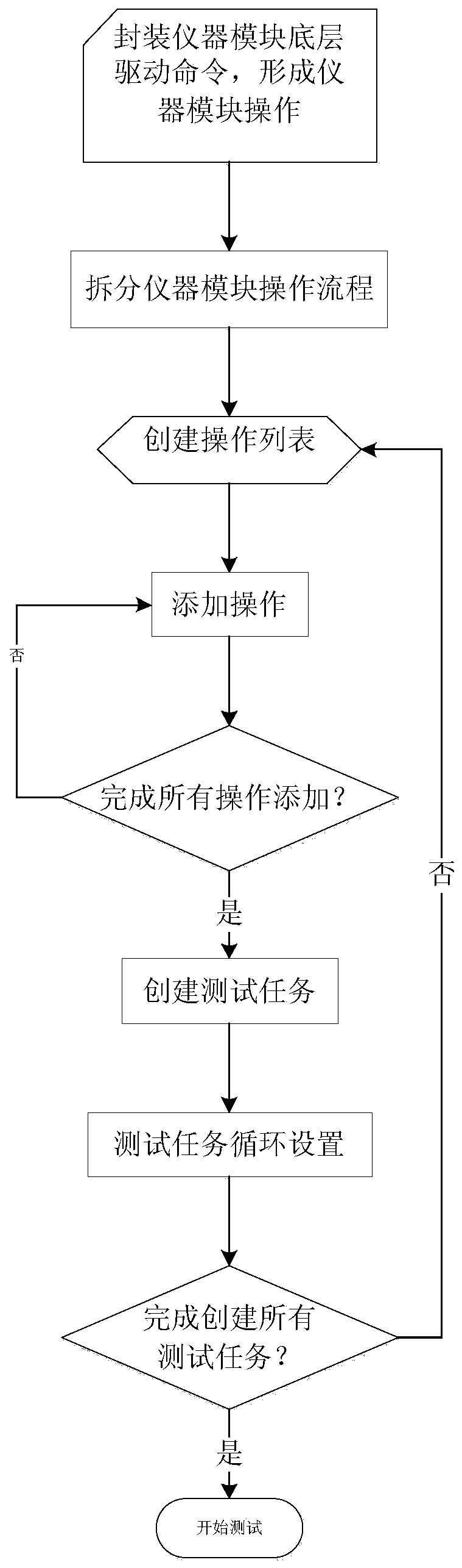
[0133] Step 1. Split testing process

[0134] Referring to the instrument module operations supported by each instrument module of the test system (see Table 1 for details), the Figure 5 The test process is split to get Image 6 Operating procedures.

[0135] Step 2. Add an instrument operation to t...

example 2

[0141] Example 2. DAC7621 laser micro-beam platform single event transient effect test

[0142] 1. Test objectives

[0143] When the DAC is tested at a stable output level, different positions of the chip are bombarded by laser pulses to capture the transient pulses generated at the output end and analyze the pulse characteristics and rules. Test process hardware interconnection such as Figure 13 shown.

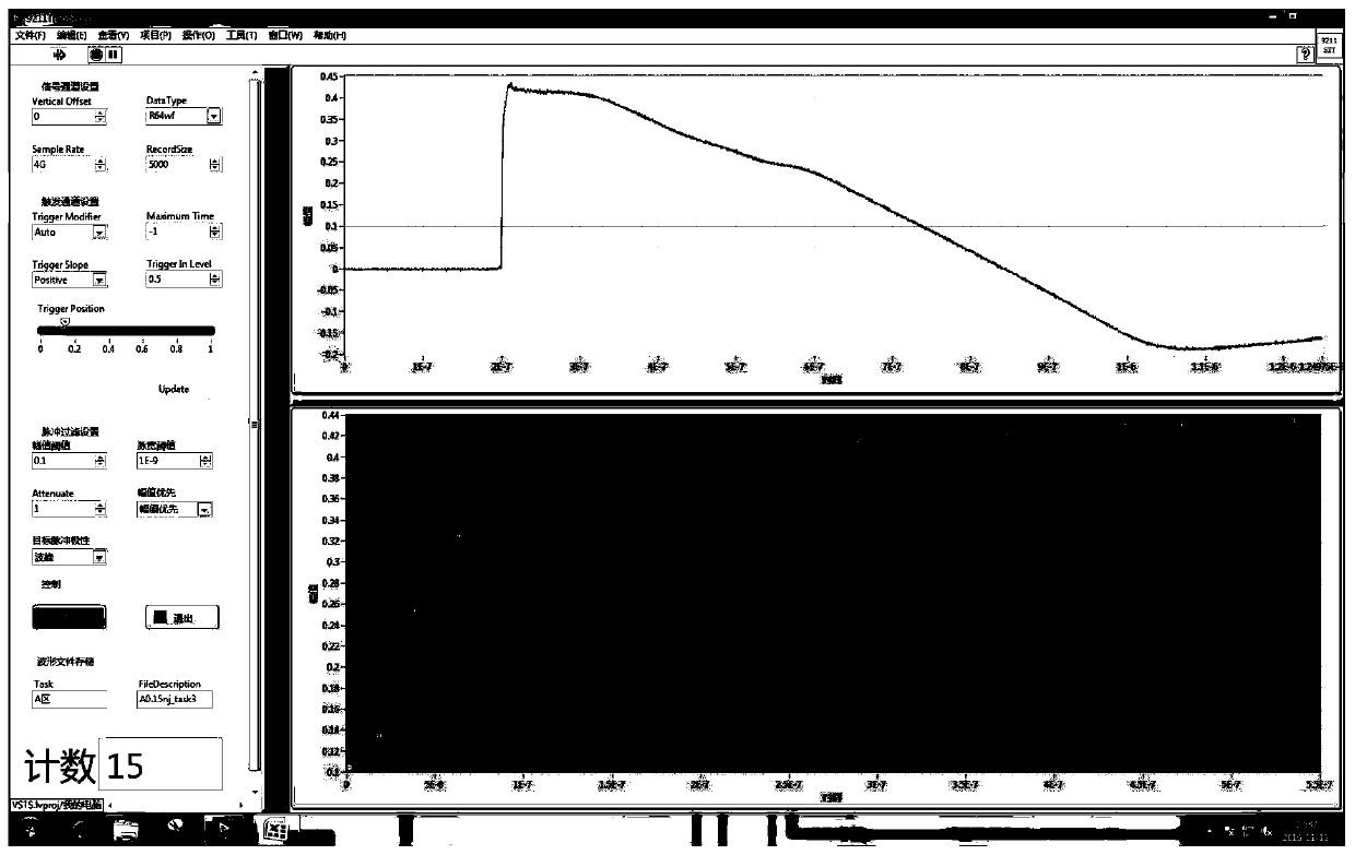
[0144] 2. Test method: The single event transient effect test maintains the output terminal at a fixed analog level by powering up the device and inputting a fixed code value. Expose the environment to the bombardment of radiating particles, and monitor the transient pulses generated on the analog signal at the output with an oscilloscope or high-speed data acquisition equipment. Because the pulse energy and bombardment position can be changed conveniently and precisely, the laser microbeam platform needs to be able to perform feature comparison and trend analysis of mult...


PUM


Abstract

The invention relates to a radiation effect general test system and a test method. The system comprises a controller, a plurality of apparatus modules, and a PXIe cabinet, and the plurality of apparatus modules comprise a high-speed digital IO, an arbitrary waveform generator, a high-speed analog acquisition card, a high-precision analog acquisition card, a matrix switch and a precision current voltage source. The method of the system mainly comprises following steps: 1) packaging bottom driving commands of all the apparatus modules to form apparatus module operations; 2) splitting an apparatus module operation process; 3) creating an operation list according to the apparatus module operation process; 4) adding the apparatus module operations; 5) creating test tasks; 6) forming a test task list; and 7) executing the test of a tested object according to the test task list. According to the system and the method, general utilization of various digital, analog, and analog-digital hybrid semiconductor device radiation effect tests can be realized, and the test precision and the test speed are obviously increased.

Description

technical field [0001] The invention belongs to the fields of radiation effect research and test and measurement, and in particular relates to a general radiation effect test system and a test method. Background technique [0002] Aerospace electronic devices work in a radiation environment composed of charged particles, and face serious threats from radiation effects, which have become one of the main sources of spacecraft reliability problems. High-energy protons, heavy ions, neutrons, and alpha particles in the space radiation environment can cause radiation effects on semiconductor electronic devices, mainly including total dose effects, single event flipping effects, single event transient effects, and single event latching effects. Affected by radiation effects, semiconductor devices will produce parameter performance degradation or device failure, which seriously affects the life and reliability of satellite electronic systems. Therefore, it is very important to eval...

Claims


Application Information

Patent Timeline
Patent Type & Authority Patents(China)
IPC IPC(8): G01R31/26
CPCG01R31/2601G01R31/2642
Inventor 刘玉辉邱孟通陈伟郭红霞郭晓强张凤祁丁李利姚志斌
Owner XIANGTAN UNIV
Why Eureka
Try Eureka