An organic electroluminescent device
An electroluminescent device and a luminescent technology, applied in the field of OLED devices, can solve problems such as harsh processes, achieve the effects of improving activity, improving device efficiency, and prolonging device life
- Summary
- Abstract
- Description
- Claims
- Application Information
AI Technical Summary
Problems solved by technology
Method used
Image
Examples
Embodiment 1
[0084] The structure of device 1:
[0085] ITO / HATCN[5nm] / NPB[30nm] / TCTA[10nm] / CBP[30nm]:10wt%Ir(ppy) 3 / Bphen[40nm] / Formula (1-3)[0.5nm] / Al[150nm]
[0086] The structure of comparative device 1 is as follows:
[0087] ITO / HATCN[5nm] / NPB[30nm] / TCTA[10nm] / CBP[30nm]:10wt%Ir(ppy) 3 / Bphen[40nm] / Al[150nm]
[0088] The structure of comparative device 2 is as follows:
[0089] The structure of this comparative example is the same as that of comparative example 1, the only difference being that the material used in the electron injection layer is LiF:
[0090] ITO / HATCN[5nm] / NPB[30nm] / TCTA[10nm] / CBP[30nm]:10wt%Ir(ppy) 3 / Bphen[40nm] / LiF[0.5nm] / Al[150nm]
[0091] Device 1, comparative device 1 and comparative device 2 have the same structure, the only difference is that the material used for the electron injection layer of device 1 is o-MeO-DMBI-I shown in formula (1-3), and the comparative device 1 has no electron injection layer material Compared with the comparative device 2...
Embodiment 2- Embodiment 5
[0096]The structure of the device 2-device 5 of the embodiment 2-the embodiment 5 is the same as that of the device 1, and the only difference lies in the thickness of the electron injection layer. Table 2 shows the performance test results.
[0097] Table 2
[0098]
[0099]
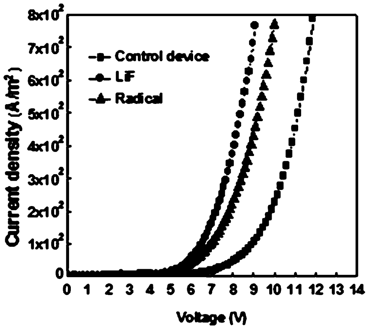
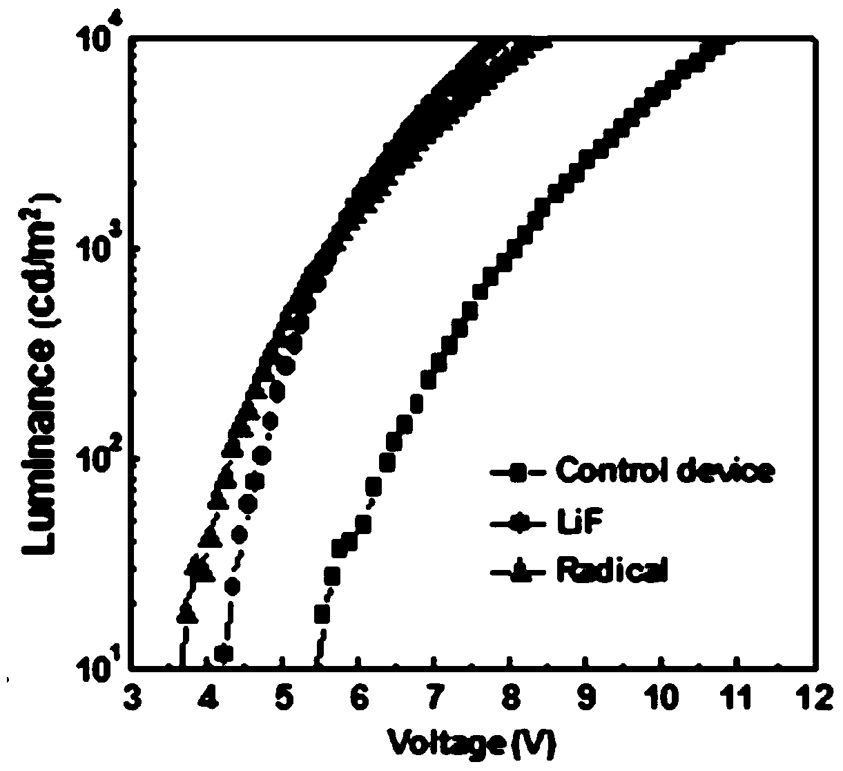
[0100] Current density of comparative device 1 (control device curve in the figure), comparative device 2 (LiF 0.5 nanometer curve in the figure) and device 1-device 5 (radical 1nm, radical 2nm, radical 3nm, radical 4nm, radical 6nm curves in the figure) - Brightness curve see Figure 6 、Current efficiency-brightness curve see Figure 7 , power efficiency-brightness curve see Figure 8 , Figure 6-Figure 8 It shows that as the thickness of the electron injection layer increases, the driving voltage gradually increases, at 35700cd / m 2 Under the luminous brightness, the maximum current efficiency first increases and then decreases with the increase of the thickness of the electron injection laye...
Embodiment 6
[0102] The structure of device 6 is the same as that of device 1, and the thickness of the electron injection layer is 3nm. The electron injection layer adopts different benzimidazole electron injection materials protected by the present invention. Table 3 shows the performance test results.
[0103] table 3
[0104]
[0105] As shown in the data in Table 3, the benzimidazole material protected by the present invention is used as an electron injection material, and the device where it is located is at 35700cd / m 2 Under the luminous brightness, it has a large current efficiency and a low driving voltage, so the benzimidazole material protected by the present invention is used as an electron injection material, so that the barrier between the cathode and the interface of the organic electron transport layer is reduced, and no longer It is necessary to set up an insulating buffer layer, which improves the transport capacity of carriers, thereby improving the efficiency of the ...
PUM
 Abstract
Description
Claims
Application Information
 - R&D
- Intellectual Property
- Life Sciences
- Materials
- Tech Scout
- Unparalleled Data Quality
- Higher Quality Content
- 60% Fewer Hallucinations
Browse by: Latest US Patents, China's latest patents, Technical Efficacy Thesaurus, Application Domain, Technology Topic, Popular Technical Reports.
© 2025 PatSnap. All rights reserved.Legal|Privacy policy|Modern Slavery Act Transparency Statement|Sitemap|About US| Contact US: help@patsnap.com


