Microimaging integrated measuring device and measuring method for optical limiting property of multi-wavelength sample

A technology of microscopic imaging and measuring device, applied in transmittance measurement and other directions, can solve problems such as accurate evaluation of unfavorable optical clipping performance, cumbersome process of changing wavelengths, and inability to observe microscopic damage on the surface of the sample, and achieve accurate measurement results. Simple operation and the effect of simplifying the measurement process

Inactive Publication Date: 2017-06-20
SHANGHAI INST OF OPTICS & FINE MECHANICS CHINESE ACAD OF SCI
View PDF7 Cites 8 Cited by
  • Summary
  • Abstract
  • Description
  • Claims
  • Application Information

AI Technical Summary

Problems solved by technology

At the same time, because the spot size keeps changing during the measurement process, it is impossible to measure the optical limiting performance of the material at a micro scale
In addition, due to the limitation of the light source, the traditional measurement method can only measure a single or a few wavelengths. The process of changing the wavelength is cumbersome, and the optical path needs to be readjusted.
(See Patent Application No.: CN201210487216, Publication No.: CN10293757

Method used


Image

  • Microimaging integrated measuring device and measuring method for optical limiting property of multi-wavelength sample
  • Microimaging integrated measuring device and measuring method for optical limiting property of multi-wavelength sample

Examples


Embodiment 1

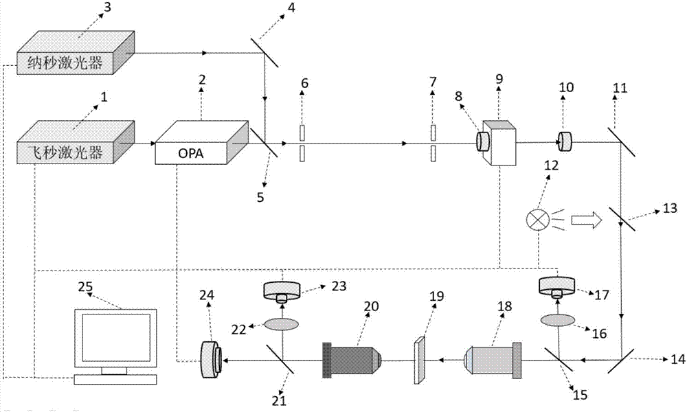
[0033] 1. According to the attached figure 1 The schematic diagram of the device shown is to build the experimental optical path, turn on the femtosecond laser, set the output light energy to 3.6uJ, and set the repetition frequency to 1KHz.

[0034] 2. Turn on the OPA device, electric rotary table, CCD and energy meter, connect them to the computer and initialize them through software in turn, and set the output wavelength of the OPA device to 515nm.

[0035] 3. Adjust the optical path of the experiment so that the outgoing laser light is incident on each optical element, and the optical elements are coaxial.

[0036] 4. Turn on the electric rotary table, energy meter Ⅰ and energy meter Ⅱ. Set the initial rotation angle and end angle of the electric turntable to 0゜ and 180゜ respectively, the angle of each rotation is set to 3゜, and the waiting time between two rotations is set to 0.5s. The single reading energy value of energy meter I17 and energy meter II23 will be set as t...


PUM

PropertyMeasurementUnit
Wavelengthaaaaaaaaaa

Abstract

The invention discloses a microimaging integrated measuring device for an optical limiting property of a multi-wavelength sample. The microimaging integrated measuring device comprises a femtosecond laser unit, an OPA device, a coating total reflective mirror II, a diaphragm I, a diaphragm II, a Glan-Taylor prism I mounted on an electric rotary table, a Glan-Taylor prism II, a coating total reflection mirror, an illuminating light source, a beam splitter I, a coating total reflective mirror IV, a beam splitter II, a focusing lens I, an energy meter I, a focusing objective lens, a collecting objective lens, a beam splitter III, a focusing lens II, an energy meter II, a CCD and a computer. The microimaging integrated measuring device realizes measuring for the wide-spectrum optical limiting property of the sample, can observe the surface topography of the optical limiting sample, the spot size of incident laser as well as sample damage condition after laser irradiation, and has the characteristics of being automatic in measuring, flexible and convenient to regulate, wide in dynamic test range, and efficient and sensitive in response speed.

Description

technical field [0001] The invention belongs to the field of optical limiting performance measurement, and in particular relates to a measuring device and method for measuring the optical limiting performance of samples with multiple wavelengths and having the function of microscopic imaging. Background technique [0002] As lasers are used more and more widely in various fields, lasers have been integrated into all aspects of people's lives. People have gradually discovered that this kind of high-intensity light source can easily damage optical devices, especially human eyes. Therefore, preventing laser damage is not only a scientific task, but also a social public safety issue. The preparation of various optical limiting materials has always been a research hotspot for scientists, and the measurement system for materials with optical limiting performance is also being continuously improved and developed. Among them, the Z-scan method is used as a means of measuring the no...

Claims


Application Information

Patent Timeline
IPC IPC(8): G01N21/59
CPCG01N21/59
Inventor 王俊王磊张赛锋李源鑫
Owner SHANGHAI INST OF OPTICS & FINE MECHANICS CHINESE ACAD OF SCI
Why Eureka
Try Eureka