Composite substrate and preparation method thereof, preparation method of light-emitting diode chip
A composite substrate and chip technology, used in semiconductor devices, electrical components, circuits, etc., can solve the problems of large warpage of epitaxial wafers, difficult to focus etching points, low yield, etc., and achieve the effect of convenient corrosion and peeling.
- Summary
- Abstract
- Description
- Claims
- Application Information
AI Technical Summary
Problems solved by technology
Method used
Image
Examples
preparation example Construction
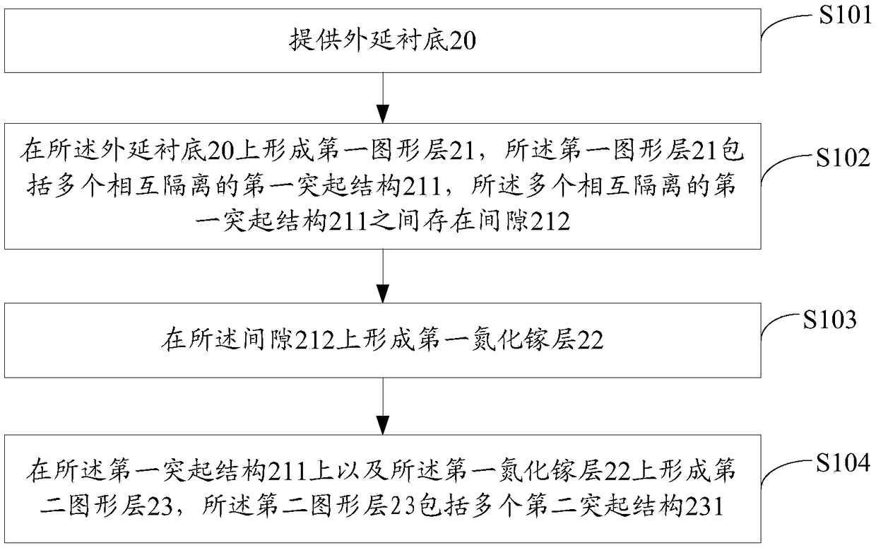
[0048] Such as figure 1 As shown, the preparation method includes the following steps:
[0049] S101. Provide an epitaxial substrate 20:
[0050] As an example, the epitaxial substrate may be a sapphire substrate. In addition, the epitaxial substrate can also be a silicon substrate, SiC and other III / V, II / VI group semiconductor substrates. Figure 2A It is a schematic diagram of the structure of the epitaxial substrate 20 provided. It should be noted that the epitaxial substrate 20 may be a substrate with a flat surface.
[0051] S102. A first patterned layer 21 is formed on the epitaxial substrate 20. The first patterned layer 21 includes a plurality of first protrusion structures 211 isolated from each other. There is a gap 212:
[0052] This step can be specifically as follows: forming a first material layer on the epitaxial substrate 20 by using technical means commonly used in the art, and then dry etching the first material layer to form the first pattern layer 21. Fig. 2B(1...
PUM
 Abstract
Description
Claims
Application Information
 - Generate Ideas
- Intellectual Property
- Life Sciences
- Materials
- Tech Scout
- Unparalleled Data Quality
- Higher Quality Content
- 60% Fewer Hallucinations
Browse by: Latest US Patents, China's latest patents, Technical Efficacy Thesaurus, Application Domain, Technology Topic, Popular Technical Reports.
© 2025 PatSnap. All rights reserved.Legal|Privacy policy|Modern Slavery Act Transparency Statement|Sitemap|About US| Contact US: help@patsnap.com


