Method used for reducing wafer edge yield test problems

A test problem, wafer technology, applied in semiconductor/solid-state device testing/measurement, electrical components, semiconductor/solid-state device manufacturing, etc., can solve the problem of low yield rate at the edge of the wafer

Active Publication Date: 2017-06-06
SHANGHAI HUAHONG GRACE SEMICON MFG CORP
View PDF6 Cites 1 Cited by
  • Summary
  • Abstract
  • Description
  • Claims
  • Application Information

AI Technical Summary

Problems solved by technology

As a result, this low yield at the wafer edge associated with test pin sticks as described above

Method used


Image

  • Method used for reducing wafer edge yield test problems
  • Method used for reducing wafer edge yield test problems
  • Method used for reducing wafer edge yield test problems

Examples


Embodiment Construction

[0025] In order to make the content of the present invention clearer and easier to understand, the content of the present invention will be described in detail below in conjunction with specific embodiments and accompanying drawings.

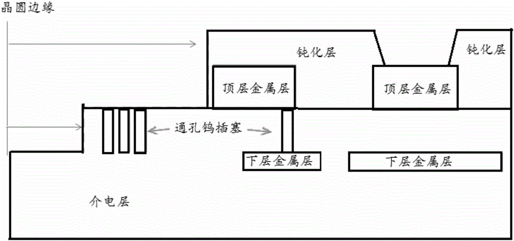
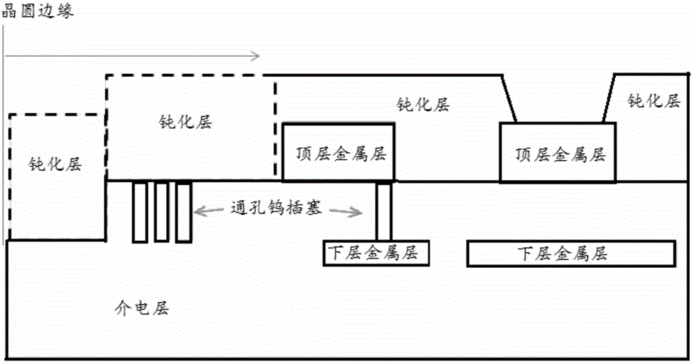
[0026] The inventors of the present invention propose that in the method for reducing the wafer edge yield test problem according to the preferred embodiment of the present invention, both the photomask and the photoresist of the passivation layer are changed into reverse phases, so that both the wafer In the circle, except the predetermined part starting from the edge position, the other part of the pattern remains unchanged; and from the edge to the predetermined part, the passivation layer remains, so that the problem of false test failure will not occur.

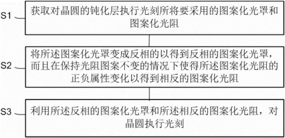
[0027] image 3 A flow chart of a method for reducing wafer edge yield test problems according to a preferred embodiment of the present invention is schematically shown.

[0028] Specific...


PUM


Abstract

The present invention provides a method used for reducing wafer edge yield test problem. The method comprises a first step of obtaining a patterned photomask and the patterned photoresist adopted to execute the photoetching on a passivation layer of a wafer; a second step of inverting the patterned photomask to obtain an inverted patterned photomask, and changing the positive and negative attributes of the patterned photoresist on the condition of keeping a constant photoresist pattern to obtain the reverse patterned photoresist; a third step of utilizing the inverted patterned photomask and the reverse patterned photoresist to execute the photoetching on the wafer. According to the method used for reducing the wafer edge yield test problems of the present invention, the photomask and the photoresist of the passivation layer both become inverted, so that the figures of other parts, except a predetermined part starting at an edge position, in the wafer, do not change, and the passivation layer is retained from the edge to the predetermined part, and accordingly, a test false failure problem is not generated.

Description

technical field [0001] The present invention relates to the fields of semiconductor manufacturing and semiconductor testing, and more particularly, the present invention relates to a method for reducing wafer edge yield testing problems. Background technique [0002] Wafer-level testing (CP Test, also known as wafer-level testing) is an important step in the semiconductor manufacturing process. Early device characterization can be obtained using wafer-level testing. [0003] However, some products will encounter the problem of low yield at the edge of the wafer when performing wafer yield testing, and even some products with a large single-chip area have a yield rate as low as 5%. This is not expected. [0004] In fact, this low wafer edge yield is related to test pin sticks. Specifically, an incomplete chip (partial die) at the edge of the wafer can cause other complete chips to be directly judged to be invalid due to leakage of electricity from the pins of the incomplet...

Claims


Application Information

Patent Timeline
Patent Type & Authority Applications(China)
IPC IPC(8): H01L21/027H01L21/66
CPCH01L21/0274H01L22/10
Inventor 王立斌邓咏桢曹秀亮康军
Owner SHANGHAI HUAHONG GRACE SEMICON MFG CORP
Why Eureka
Try Eureka