Circuit board packaging structure and manufacturing method thereof

A technology of packaging structure and manufacturing method, which is applied in the manufacture of printed circuits, printed circuits, and assembling printed circuits with electrical components. Yield effect

Active Publication Date: 2017-05-31
TRIPOD WUXI ELECTRONICS
View PDF6 Cites 0 Cited by
  • Summary
  • Abstract
  • Description
  • Claims
  • Application Information

AI Technical Summary

Problems solved by technology

However, with the miniaturization of the package structure of the circuit board, the size of the conductive through hole is gradually reduced, making the manufacturing process more difficult and prone to uneven plating.

Method used


Image

  • Circuit board packaging structure and manufacturing method thereof
  • Circuit board packaging structure and manufacturing method thereof
  • Circuit board packaging structure and manufacturing method thereof

Examples


Embodiment Construction

[0043] The aforementioned and other technical contents, features and effects of the present invention will be clearly presented in the following detailed descriptions of the embodiments with reference to the accompanying drawings. The directional terms mentioned in the following embodiments, such as: "upper", "lower", "front", "rear", "left", "right", etc., are only referring to the directions of the attached drawings. Accordingly, the directional terms used are illustrative, not limiting, of the invention. Also, in the following embodiments, the same or similar components will be given the same or similar symbols.

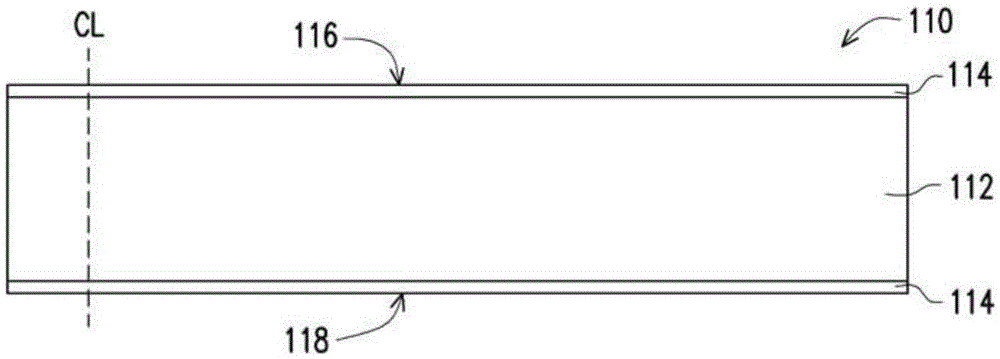
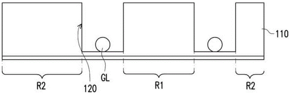
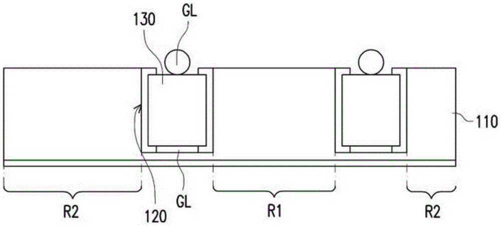
[0044] Figure 1A to Figure 1M is a schematic cross-sectional flow diagram of a manufacturing method of a circuit board packaging structure according to an embodiment of the present invention. Please refer to Figure 1A , The manufacturing method of the circuit board packaging structure of this embodiment includes the following steps. First, provide the Figur...


PUM


Abstract

The present invention discloses a circuit board packaging structure and a manufacturing method thereof. The circuit board packaging structure comprises a substrate, an annular magnetic element, a first stack-up layer, a plurality of external conduction columns, a plurality of internal conduction columns, a plurality of second stack-up layers and a plurality of conductive slots. The substrate comprises an annular groove, and a first surface and a second surface which are opposite with each other. The annular groove is arranged at the first surface. The annular magnetic element is arranged in the annular groove. The first stack-up layer is arranged on the first surface. The external conduction columns and the internal conduction columns run through the substrate and are respectively located at the external area and the internal area of the annular groove. The external conduction columns are electrically connected with the corresponding internal conduction columns. The second stack-up layers are respectively arranged on the first stack-up layers and the second surface. The conductive slots are arranged at the periphery of the substrate. The conductive slots run through the substrate, the first stack-up layer and the second stack-up layer.

Description

technical field [0001] The invention relates to a semiconductor packaging structure and a manufacturing method of the semiconductor packaging structure, and in particular to a circuit board packaging structure and a manufacturing method of the circuit board packaging structure. Background technique [0002] Generally speaking, during the manufacturing process of the circuit board, specific components, such as copper blocks and iron cores for heat dissipation, need to be placed into the predetermined accommodation slots of the circuit board. The iron core can be applied to the structure of a transformer or a choke because of its magnetic properties. The magnetic element is very sensitive to stress, and the electrical characteristics of the magnetic element will be affected by the stress caused by the environment and even cause damage. The existing manufacturing process and packaging structure itself will produce stress that affects the inductance value. [0003] The existing...

Claims


Application Information

Patent Timeline
Patent Type & Authority Applications(China)
IPC IPC(8): H05K3/30
CPCH05K3/30H05K2203/1316
Inventor 黄柏雄杨伟雄石汉青林正峰
Owner TRIPOD WUXI ELECTRONICS
Why Eureka
Try Eureka