
A high-power silicon-based tunable external cavity laser with dual-port output

A laser, dual-port technology, used in lasers, laser parts, semiconductor lasers, etc., can solve the uneven gain of long and short wavelengths, increase the process control accuracy requirements and processing difficulties of silicon-based micro-ring waveguide chips, and small differences in free spectral range. and other problems, to achieve the effect of expanding the limit optical power, reducing the control accuracy of the manufacturing process, and being easy to mass-produce

Active Publication Date: 2020-07-28
GUANGXUN SCI & TECH WUHAN
View PDF2 Cites 0 Cited by
  • Summary
  • Abstract
  • Description
  • Claims
  • Application Information

AI Technical Summary

Problems solved by technology

Generally speaking, when the spectral width of the SOA gain spectrum is larger than the C Band, its long-wavelength and short-wavelength gains will also have obvious unevenness. Existing tunable lasers use a double-ring silicon-based chip directly connected to the SOA structure, which must be theoretically designed. Ensure that the free spectral range (FSR: Free Spectrum Range) of the synthetic spectrum of the silicon-based chip double-ring vernier effect is greater than the C Band, that is, the two micro-ring filters are required to have a larger free spectral range and a smaller free spectral range difference, so that As a result, the process control accuracy requirements and processing difficulty of silicon-based microring waveguide chip production will be greatly increased

Method used

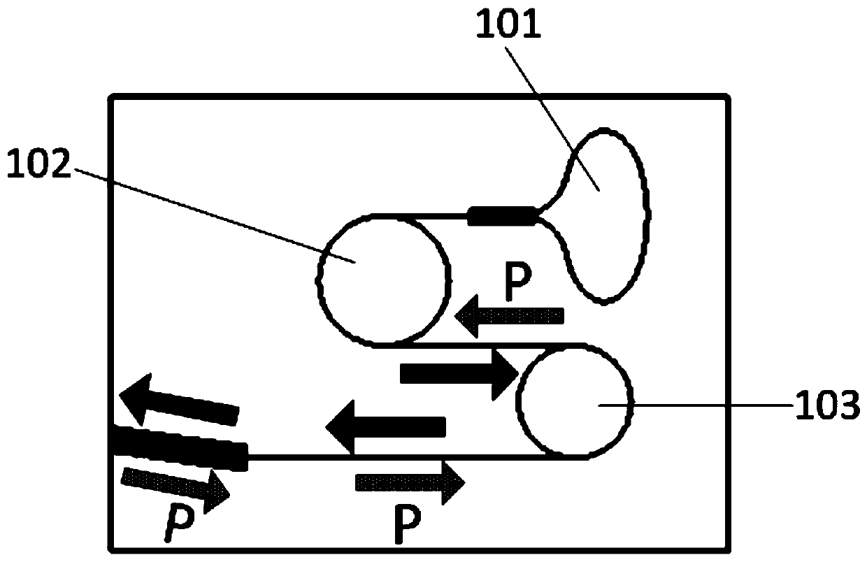
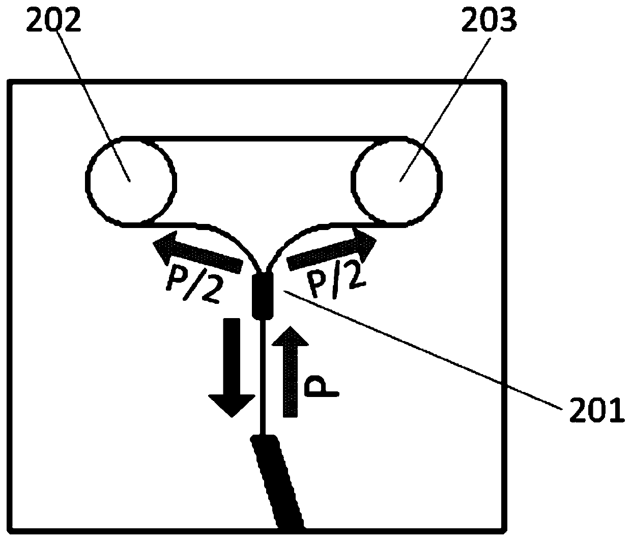

Image

  • A high-power silicon-based tunable external cavity laser with dual-port output
  • A high-power silicon-based tunable external cavity laser with dual-port output
  • A high-power silicon-based tunable external cavity laser with dual-port output

Examples


Embodiment Construction

[0044] In order to make it easier for those skilled in the art to understand and implement the present invention, the present invention will be further described in detail below in conjunction with the accompanying drawings and specific embodiments.

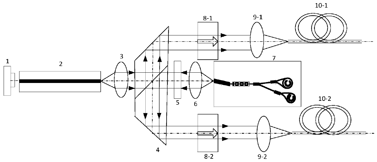
[0045] The silicon-based tunable external cavity laser with high-power dual-port output provided by the present invention, such as image 3 As shown, it includes a photodetector 1, a reflective semiconductor gain chip 2 (RSOA: Reflective Semiconductor Optical Amplifier), a collimator lens 3, an optical beam splitter 4, a bandpass filter 5, a waveguide coupling lens 6, and a silicon-based microring Chip 7, first and second port optical isolators 8-1 and 8-2, first and second port output coupling lenses 9-1 and 9-2 and first and second port output optical fibers 10-1 and 10 -2. Wherein, the reflective semiconductor gain chip 2 is used to provide gain, and its two ends are respectively coated with a high reflection film and an anti...


PUM


Abstract

The invention relates to a high-power dual-port output silicon-based tunable external cavity laser. A hybrid integration scheme is adopted, a low-cost low-loss silicon-based microring waveguide chip is used as an external cavity medium wavelength adjustment unit, end surface coupling with an III-V group reflective semiconductor gain tube core is realized through two collimating lenses, the structure is simple, the complex process limitations of a monolithic integrated semiconductor laser are overcome, no moving part exists in the external cavity, and the reliability and the stability can be effectively improved. Through optimal design of the silicon-based microring waveguide chip structure, the nonlinear optical effect generation probability of laser in a silicon-based waveguide microring resonator is greatly reduced, and the maximum optical power which is allowed to be outputted by the laser of the structure is improved. Due to addition of a band pass filter in the external cavity collimating light path, technical requirements on the silicon-based microring waveguide chip can be effectively reduced, the coupling packaging efficiency can be improved, and low-cost batch production is facilitated.

Description

technical field [0001] The invention relates to an optical communication device, in particular to a high-power dual-port output silicon-based tunable external cavity laser, in particular to a laser gain chip of the III-V family and a silicon-based microring optical waveguide The invention discloses a realization scheme of a chip hybrid integrated dual-port output external cavity tunable laser, the tunable external cavity laser is suitable for a coherent optical communication network with a flexible wavelength grid, and belongs to the technical field of optical communication. Background technique [0002] Coherent optical communication technology has many advantages such as high receiving sensitivity bandwidth, long relay distance, good wavelength selectivity, and large communication capacity. In recent years, it has gradually become the main technology of trunk transmission network. In high-speed coherent communication systems, high-performance tunable lasers are indispensab...

Claims


Application Information

Patent Timeline
Patent Type & Authority Patents(China)
IPC IPC(8): H01S5/00H01S5/06H01S5/14
CPCH01S5/0071H01S5/0078H01S5/06H01S5/141H01S5/1032H01S5/142
Inventor 汤学胜陈义宗钱坤胡毅曹薇焰烽马卫东
Owner GUANGXUN SCI & TECH WUHAN
Learn More