Two-dimensional photonic crystal plate structure band gap design method based on wavelet finite element model
A two-dimensional phononic crystal and wavelet finite element technology, applied in design optimization/simulation, calculation, special data processing applications, etc., can solve problems such as low precision, slow convergence, and constraints on the bandgap design of phononic crystal plate structures , to achieve the effects of high calculation accuracy, good calculation efficiency and convergence
- Summary
- Abstract
- Description
- Claims
- Application Information
AI Technical Summary
Problems solved by technology
Method used
Image

Examples
Embodiment 1
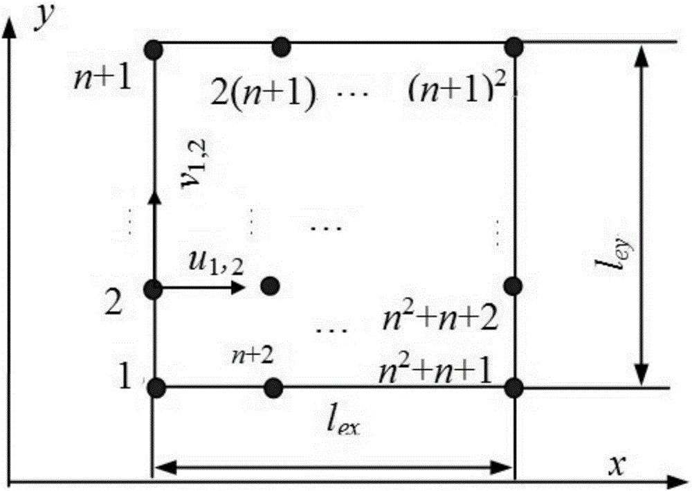
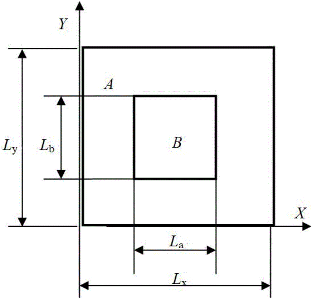
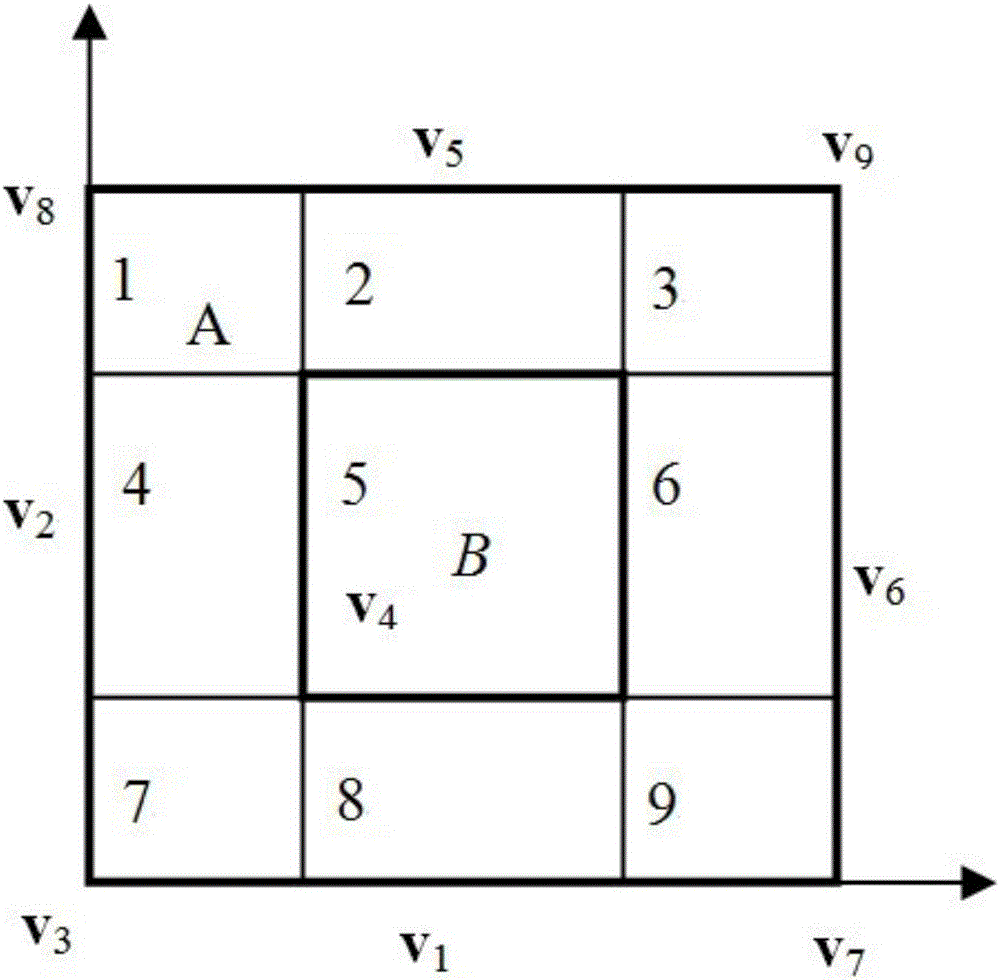
[0107] Embodiment 1: This embodiment mainly verifies the calculation accuracy of the wavelet finite element numerical solution model for calculating the band gap of the two-dimensional phononic crystal plate structure. In order to verify the correctness and effectiveness of the constructed BSWI plate element in the calculation of the bandgap of the phononic crystal, this section will give an example verification. As shown in Figure 2, the scatterers are periodically arranged in rectangular lead plates (Part B) and embedded in the epoxy resin (Part A) matrix to form a two-dimensional phononic crystal plate, and the filling rate is f=(L a × L b ) / (L x × L y )=11%, limited lattice constant Lx with L y Both are equal to 0.03m. For the material parameters of lead and epoxy resin, see Image 6 .
[0108] First use 9 (m=3, n=3) BSWI4 3 The plate unit is used to calculate the bandgap characteristics of the two-dimensional phononic crystal. The BSWI scaling function used here is ...
Embodiment 2
[0109] Embodiment 2: This embodiment mainly verifies the calculation efficiency of the wavelet finite element numerical solution model for calculating the band gap of a two-dimensional rectangular plate phononic crystal. Rectangular plates are also widely used in engineering practice as structural components. This paper will use BSWI wavelet finite element method to study the band gaps of phononic crystals with different lattice forms. For material parameters of lead and epoxy resin, see Image 6 .
[0110] We use a rectangular lattice to study the effect of the bandgap of phononic crystals, where L x not equal to L y . The corresponding structural parameters are: L x =0.03m, L y = 0.02m, L a =L b =0.01m, filling rate f=16.7%. 9 BSWI4 respectively 3 Plate unit (m=3, n=3), 20×20, 40×40 traditional rectangular plate units to calculate the band gap of phononic crystal, the results are shown in Figure 4 , the results are represented by dots, solid lines, and square boxe...
Embodiment 3
[0111] Embodiment 3: This embodiment mainly provides the scale range of the phononic crystal structure of a two-dimensional rectangular plate with a relatively wide bandgap calculated by using the wavelet finite element model. For material parameters of lead and epoxy resin, see Image 6 . Without loss of generality, the fixed structure parameters are: L x =0.03m, L y = 0.02m.
[0112] Adopt 9 BSWI4 3 Plate elements (m=3, n=3) are used to calculate the bandgap of phononic crystals. In order to obtain the bandgap characteristics that meet the requirements of a specific frequency band, the structural size of the two-dimensional phononic crystal plate is continuously calculated and adjusted. Under the premise of fixing the lattice constant, the relationship between the geometric dimensions of the scatterer is determined by obtaining the best filling rate, and finally the two-dimensional phononic crystal plate is completed. The bandgap design of the two-dimensional phononic c...
PUM
 Abstract
Description
Claims
Application Information
 - Generate Ideas
- Intellectual Property
- Life Sciences
- Materials
- Tech Scout
- Unparalleled Data Quality
- Higher Quality Content
- 60% Fewer Hallucinations
Browse by: Latest US Patents, China's latest patents, Technical Efficacy Thesaurus, Application Domain, Technology Topic, Popular Technical Reports.
© 2025 PatSnap. All rights reserved.Legal|Privacy policy|Modern Slavery Act Transparency Statement|Sitemap|About US| Contact US: help@patsnap.com