Flexible fully-inorganic QLED device and preparation method thereof
An inorganic and device technology, which is applied in the field of flexible all-inorganic QLED devices and its preparation, can solve the problems of low crystallinity, many structural defects, and low carrier transport efficiency of the hole transport layer, and achieve less crystal defects and rough interfaces Small degree, the effect of improving carrier transport efficiency
- Summary
- Abstract
- Description
- Claims
- Application Information
AI Technical Summary
Problems solved by technology
Method used
Image
Examples
Embodiment 1
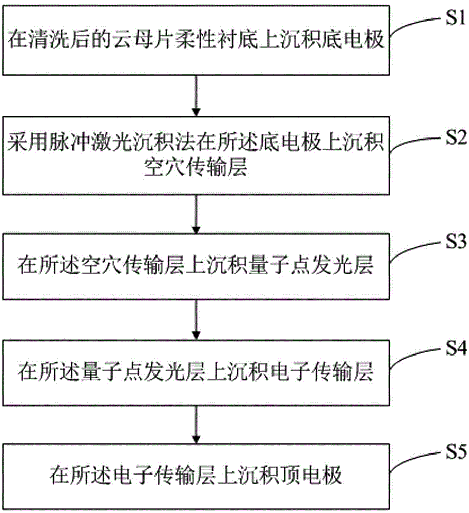
[0056] (1) First, clean the mica slices, and place them in ultrapure water, acetone water, and isopropanol for ultrasonic cleaning in sequence. The time for each step of ultrasonic cleaning is 15 minutes. Dry it with a gun, place it in an oven to dry, and obtain the flexible substrate of the mica sheet after cleaning for future use;
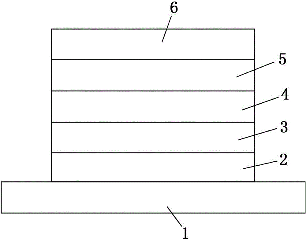
[0057] (2) On the cleaned mica sheet flexible substrate, a layer of patterned ITO electrode, that is, the bottom electrode, is sputtered and deposited on it through a mask plate, and the thickness of the ITO electrode is 60 nm;
[0058] (3) A 50-nm-thick hole-transporting layer WO was deposited on the ITO electrode using laser pulses 3 , before deposition, pump the deposition chamber to 1×10 -5 Base pressure of Torr; by KrF excimer laser (maximum energy 650mJ, λ=248nm, pulse duration 25ns) at 2J / cm 2 The energy density, frequency of 5Hz ablate stoichiometric WO 3 Target 10min (the number of pulses is 3000); among them, the distance between the...
Embodiment 2
[0063] (1) First, clean the mica slices, and place them in ultrapure water, acetone water, and isopropanol for ultrasonic cleaning in sequence. The time for each step of ultrasonic cleaning is 15 minutes. Dry it with a gun, place it in an oven to dry, and obtain the flexible substrate of the mica sheet after cleaning for future use;
[0064] (2) On the cleaned mica sheet flexible substrate, a layer of patterned ITO electrode, that is, the bottom electrode, is sputtered and deposited on it through a mask plate, and the thickness of the ITO electrode is 60 nm;
[0065] (3) Deposit a layer of 50nm thick hole transport layer NiO on the ITO electrode using laser pulses. Before deposition, pump the deposition chamber to 1×10 -5 Base pressure of Torr; by KrF excimer laser (maximum energy 650mJ, λ=248nm, pulse duration 25ns) at 2J / cm 2 The energy density, the frequency of 5Hz ablate the stoichiometric NiO target for 15min (the number of pulses is 4500); the distance between the targe...
PUM
| Property | Measurement | Unit |
|---|---|---|
| Thickness | aaaaa | aaaaa |
| Thickness | aaaaa | aaaaa |
| Thickness | aaaaa | aaaaa |
Abstract
Description
Claims
Application Information
 - R&D
- Intellectual Property
- Life Sciences
- Materials
- Tech Scout
- Unparalleled Data Quality
- Higher Quality Content
- 60% Fewer Hallucinations
Browse by: Latest US Patents, China's latest patents, Technical Efficacy Thesaurus, Application Domain, Technology Topic, Popular Technical Reports.
© 2025 PatSnap. All rights reserved.Legal|Privacy policy|Modern Slavery Act Transparency Statement|Sitemap|About US| Contact US: help@patsnap.com


