Method for metal configuration with photoresist deposition
A technology for depositing metal and photoresist, which is used in the manufacture of electrical components, circuits, semiconductor/solid-state devices, etc., and can solve problems such as side corrosion and metal residues
- Summary
- Abstract
- Description
- Claims
- Application Information
AI Technical Summary
Problems solved by technology
Method used
Image


Examples
Embodiment 1
[0069] A method of depositing a metal pattern using a photoresist, comprising:
[0070] A step of coating photoresist on the surface of the substrate;
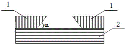
[0071] The above substrate coated with photoresist is sequentially subjected to the steps of baking, exposure, baking and development, and the angle between the side wall of the photoresist pattern obtained after development and the surface of the substrate is between 80° and 100° between;
[0072] The step of depositing metal onto the surface of the developed photoresist pattern, and the metal falls on the surface of the substrate at the opening of the photoresist;
[0073] The step of removing the metal on the surface of the above-mentioned photoresist;
[0074] The step of removing the photoresist.
[0075] Preferably, after the above-mentioned photoresist-coated substrate is sequentially subjected to the steps of baking, exposure, baking and development, it also includes the step of corroding the thin layer on the surfa...
Embodiment 2
[0089] Place the 2-inch sapphire wafer that has been patterned and epitaxial GaN into the rotary coating machine manually, drop about 2 ml of soluble negative photoresist, start the coating coating machine, 3000 revolutions per minute, and last for 60 seconds Rear. Bake at 110°C for 60 seconds on a hot plate, then cool to room temperature. The photoresist film thickness was measured with a Dektak XT profilometer to be 2.35 microns. Use a proximity type (US SUSS exposure machine MA-100E) exposure machine to expose at a gap of 10 microns, and the exposure light source uses a high-pressure mercury lamp mixed wavelength light source. The mask board is an LED electrode pattern with finger. Then bake at 110 degrees Celsius for 60 seconds using a hot plate and then let it cool down to room temperature. Soak in 2.38% tetramethyl ammonium hydroxide developer solution for 60 seconds and rinse with deionized water. Such as Figure 8a Shown is a cross-sectional electron microscope pi...
Embodiment 3
[0091] Place the 2-inch sapphire wafer that has been patterned and epitaxially GaN into the rotary coating machine manually, drop about 2 ml of soluble negative photoresist to start the coating machine, 4000 rotations per minute, and continue to use for 60 seconds The hot plate is baked at 110°C for 60 seconds and then cooled to room temperature. The photoresist film thickness was measured with a Dektak XT profilometer to be 1.50 microns. Exposure, baking and development were performed using the process of Example 2. Figure 9a It is a cross-sectional electron microscope picture of the obtained photoresist pattern, the width of the groove is 5.0 microns, and the side wall of the photoresist pattern is perpendicular to the surface of the substrate. Etch with BOE (Buffer Oxide Etcher) for 40 seconds at room temperature. Metal gold was evaporated in ei-5z high vacuum evaporation coating equipment (ULVAC, Japan) for 5 hours. Figure 9b It is a cross-sectional electron microscop...
PUM
| Property | Measurement | Unit |
|---|---|---|
| Thickness | aaaaa | aaaaa |
| Thickness | aaaaa | aaaaa |
Abstract
Description
Claims
Application Information
 - R&D
- Intellectual Property
- Life Sciences
- Materials
- Tech Scout
- Unparalleled Data Quality
- Higher Quality Content
- 60% Fewer Hallucinations
Browse by: Latest US Patents, China's latest patents, Technical Efficacy Thesaurus, Application Domain, Technology Topic, Popular Technical Reports.
© 2025 PatSnap. All rights reserved.Legal|Privacy policy|Modern Slavery Act Transparency Statement|Sitemap|About US| Contact US: help@patsnap.com