Radio-frequency switch circuit

A radio frequency switch and circuit technology, applied in electronic switches, electrical components, pulse technology, etc., can solve problems such as unbalanced voltage distribution

Active Publication Date: 2017-05-10
SHANGHAI HUAHONG GRACE SEMICON MFG CORP
View PDF8 Cites 1 Cited by
  • Summary
  • Abstract
  • Description
  • Claims
  • Application Information

AI Technical Summary

Problems solved by technology

[0004] With the development of modern radar and radio communication technologies, various electronic devices have continuously put forward higher requirements for the RF switch circuits used in their internal applications or system tests. One of the important points is that the existing RF switch circuits make the voltage distribution uneven. balance, which seriously affects the power handling capability and even causes the high voltage on the transistor to break down the transistor. Therefore, it is necessary to improve the structure of the existing RF switch circuit, reduce the maximum voltage difference distributed between the source and drain of the transistor, and reduce the size of the transistor Risk of breakdown by high voltage

Method used


Image

  • Radio-frequency switch circuit
  • Radio-frequency switch circuit
  • Radio-frequency switch circuit

Examples


Embodiment 1

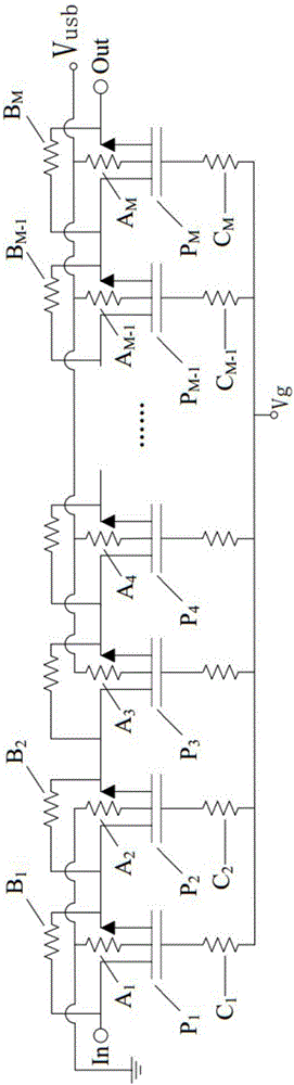
[0026] The invention provides a radio frequency switch circuit, the specific structure is as follows figure 2 As shown, the radio frequency switch circuit includes a transistor chain composed of M transistor connections, and the transistor chain includes a first transistor P 1 , the second transistor P 2 , the third transistor P 3 , the fourth transistor P 4 , ..., the M-1th transistor P M-1 and the Mth transistor P M , used to control radio frequency signals in electronic circuits.

[0027] Wherein, the first transistor P 1 the substrate and the second transistor P 2 The substrates are respectively grounded through different first resistors. Specifically, the first transistor P 1 The substrate is connected with a first first resistor A 1 , the second crystal P 2 The substrate is connected with a second first resistor A 2 , the first first resistor A 1 with the second first resistor A 2 connected in series and grounded.

[0028] The third transistor P 3 , the f...

Embodiment 2

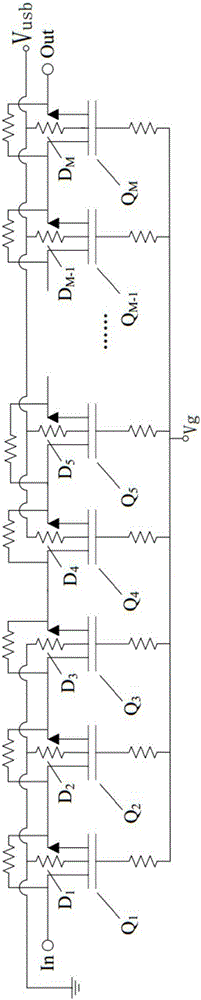
[0036] The invention provides a radio frequency switch circuit, the specific structure is as follows image 3 As shown, it includes a transistor chain composed of M transistor connections, and the transistor chain includes a first transistor Q 1 , the second transistor Q 2 , the third transistor Q 3 , the fourth transistor Q 4 , the fifth transistor Q 5 , ..., the M-1th transistor Q M-1 and the Mth transistor Q M , used to control radio frequency signals in electronic circuits.

[0037] Wherein, the first transistor Q 1 The substrate, the second transistor Q 2 substrate and the third transistor Q 3 The substrates are respectively grounded through different first resistors. Specifically, the first transistor Q 1 The substrate is connected with a first first resistor D 1 , the second crystal Q 2 The substrate is connected with a second first resistor D 2 , the third transistor Q 3 connected with a third first resistor D 3 , the first first resistor D 1 , the seco...


PUM


Abstract

The present invention provides a radio-frequency switch circuit, which comprises a transistor chain formed through the connection of M transistors. The transistor chain comprises a first transistor, a second transistor, a third transistor,.., a M-1 transistor and a M transistor. The substrate of the first transistor and the substrate of the second transistor are grounded respectively through different first resistors. The substrates of the rest M-2 transistors are connected with a first negative bias respectively through different first resistors. The invention also provides another radio-frequency switch circuit, wherein the substrate of the first transistor, the substrate of the second transistor and the substrate of the third transistor are grounded respectively through different first resistors and the substrates of the rest M-3 transistors are connected with the first negative bias respectively through different first resistors. The above two radio-frequency switch circuits can reduce the maximum differential pressure between the source and the drain of a transistor, so that the voltage on the transistor is more evenly distributed.

Description

technical field [0001] The invention relates to the technical field of semiconductor circuits, in particular to a radio frequency switch circuit. Background technique [0002] The RF switch is one of the control devices used to control the transmission path and signal size of the RF signal. It is widely used in many fields such as wireless communication, electronic countermeasures, radar systems, and electronic measuring instruments. [0003] The existing RF switch circuit is composed of M transistor connections, such as figure 1 As shown, from left to right are the first transistor 1, the second transistor 2, the third transistor 3...the M-1th transistor M-1 and the Mth transistor M. The drain of the first transistor 1 is used as the input terminal of the radio frequency switch circuit, and its source is connected with the drain of the second transistor 2; the source of the second transistor 2 is connected with the drain of the third transistor 3 The poles are connected.....

Claims


Application Information

Patent Timeline
Patent Type & Authority Applications(China)
IPC IPC(8): H03K17/081
CPCH03K17/081
Inventor 刘张李
Owner SHANGHAI HUAHONG GRACE SEMICON MFG CORP
Why Eureka
Try Eureka