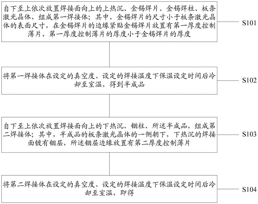
Double-sided packaging method of slab laser crystal
A laser crystal and packaging method technology, applied in the field of lasers, can solve the problems of aggravating thermal effects, large-area virtual welding, affecting the beam quality and reliability of solid-state lasers, etc., and achieves the effect of eliminating air and reducing the generation of holes
- Summary
- Abstract
- Description
- Claims
- Application Information
AI Technical Summary
Problems solved by technology
Method used
Image
Examples
example 1
[0037] The double-sided encapsulation method of slab laser crystal in the example 1 comprises the following steps:
[0038] (1) From bottom to top, heat sink 1, gold-tin solder sheet and aluminum alloy thickness control sheet, gold-tin solder column, Nd:YAG slab laser crystal are placed in sequence from bottom to top, and the welding body 1 is composed of the above; the Nd: The size of the YAG slab laser crystal is 3mm×40mm×140mm, the optical film thickness of the Nd:YAG slab laser crystal is 4μm, the metal titanium film thickness is 300nm, the platinum film thickness is 300nm, and the gold film thickness is 800nm; The thickness of the sheet is 120μm, and the area is 38mm×126mm; the thickness of the aluminum alloy thickness control sheet is 80μm, the height of the gold-tin soldering post is 120μm; the thickness of the heat-sink gold film is 500nm.
[0039] (2) Put the welding body 1 into the vacuum welding furnace, and evacuate the vacuum welding furnace to 6×10 -3 Pa, the we...
example 2
[0043] The double-sided encapsulation method of slab laser crystal in the example 1 comprises the following steps:
[0044] (1) Place the heat sink 1 with the welding surface upward, the gold-tin solder sheet and the aluminum alloy thickness control sheet, the gold-tin solder column, and the Yb:YAG slab laser crystal from bottom to top, and the above constitute the welded body 1; where Yb:YAG The size of the slab laser crystal is 1.3mm×10mm×50mm, the optical film thickness of the Yb:YAG slab laser crystal is 3μm, the metal titanium film thickness is 100nm, the platinum film thickness is 300nm, and the gold film thickness is 500nm. The thickness of the gold-tin solder sheet is 100 μm, and the area is 9mm×48mm; the thickness of the aluminum alloy thickness control sheet is 60 μm; the height of the gold-tin solder column is 120 μm; the thickness of the heat-sink gold film is 400nm.
[0045] (2) Put the welding body 1 into the vacuum welding furnace, and evacuate the vacuum weldin...
PUM
| Property | Measurement | Unit |
|---|---|---|
| thickness | aaaaa | aaaaa |
| thickness | aaaaa | aaaaa |
| height | aaaaa | aaaaa |
Abstract
Description
Claims
Application Information
 - R&D Engineer
- R&D Manager
- IP Professional
- Industry Leading Data Capabilities
- Powerful AI technology
- Patent DNA Extraction
Browse by: Latest US Patents, China's latest patents, Technical Efficacy Thesaurus, Application Domain, Technology Topic, Popular Technical Reports.
© 2024 PatSnap. All rights reserved.Legal|Privacy policy|Modern Slavery Act Transparency Statement|Sitemap|About US| Contact US: help@patsnap.com


