High-efficiency preparation method for nitrogen-doped titanium dioxide film
A titanium dioxide and nitrogen doping technology is applied in the field of photocatalytic materials to achieve the effects of good photocatalytic effect, high film quality and fast deposition rate
- Summary
- Abstract
- Description
- Claims
- Application Information
AI Technical Summary
Problems solved by technology
Method used
Image
Examples
Embodiment 1
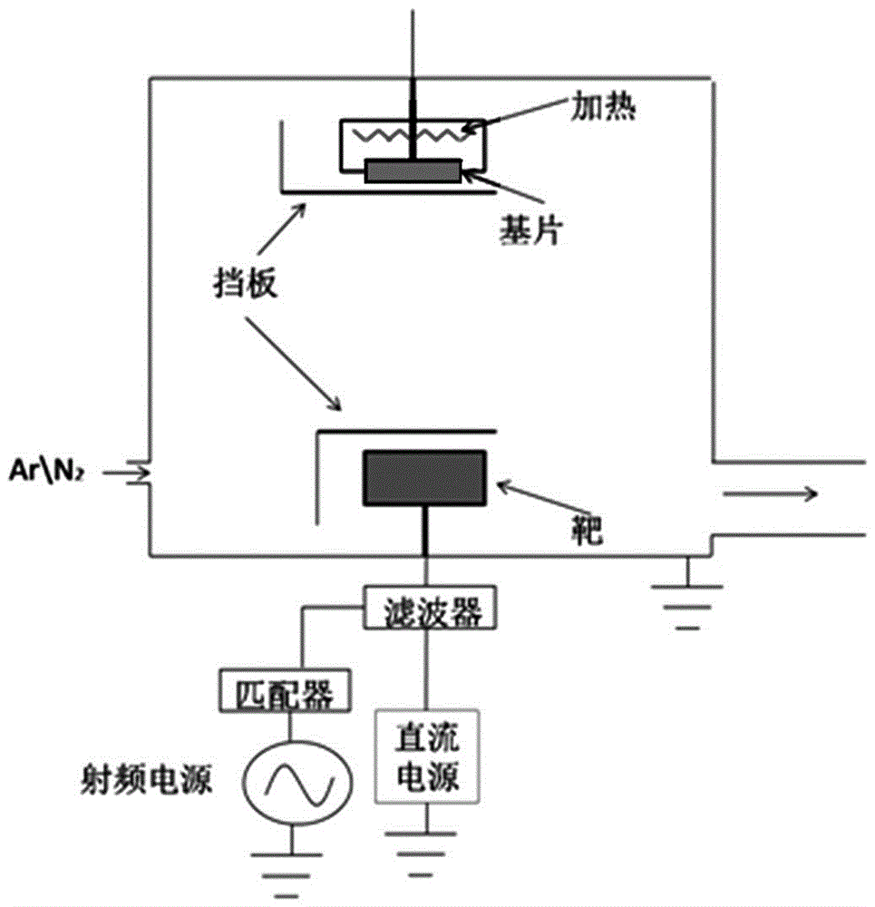
[0026] Such as figure 1 As shown, in the magnetron sputtering chamber, the glass substrate is set on the anode, TiO 2 The ceramic target is set on the cathode, the RF power supply is connected to the matcher and then connected to the filter together with the DC power supply, and the filter is directly connected to the cathode. The RF power and the DC power together supply power to the cathode.
[0027] A high-efficiency nitrogen-doped titanium dioxide film according to the present invention is prepared through the following steps:
[0028] (1) Cleaning of the surface of the glass substrate: select a glass substrate with a thickness of 1.1mm and put it into an ultrasonic cleaner, first use acetone for 20 minutes, then use alcohol for 20 minutes, and finally use deionized water for 20 minutes. 2 blow dry.
[0029] (2) Take out the glass substrate and put it into the magnetron sputtering equipment (anode), target (cathode): TiO 2 Ceramic target (99.99% pure);
[0030] The pr...
Embodiment 2
[0039] (1) Cleaning of the surface of the glass substrate: select a glass substrate with a thickness of 0.7mm and put it into an ultrasonic cleaning machine, first use acetone for 20 minutes, then use alcohol for 20 minutes, and finally use deionized water for 20 minutes, and use high-pressure N 2 blow dry.
[0040] (2) Take out the glass substrate and put it into a magnetron sputtering device to deposit a nitrogen-doped titanium dioxide film. The preparation process parameters are as follows:
[0041] Target material: TiO 2 Ceramic target (purity: 99.99%)
[0042] Background vacuum≤8×10 -4 Pa;
[0043] Working pressure: 6×10 -1 Pa;
[0044] DC sputtering power: 75W;
[0045] RF sputtering power: 175W;
[0046] Sputtering process gas Ar flow: 25sccm;
[0047] Reactive gas N 2 Flow rate: 6 sccm;
[0048] Deposition coating thickness: 500nm.
PUM
 Abstract
Description
Claims
Application Information
 - R&D Engineer
- R&D Manager
- IP Professional
- Industry Leading Data Capabilities
- Powerful AI technology
- Patent DNA Extraction
Browse by: Latest US Patents, China's latest patents, Technical Efficacy Thesaurus, Application Domain, Technology Topic, Popular Technical Reports.
© 2024 PatSnap. All rights reserved.Legal|Privacy policy|Modern Slavery Act Transparency Statement|Sitemap|About US| Contact US: help@patsnap.com


