Method of electroplating copper into a via on a substrate from an acid copper electroplating bath
A technology of copper electronics and substrates, which is applied to circuits, electrical components, semiconductor devices, etc., and can solve problems such as surface defects of unresolved copper deposits
- Summary
- Abstract
- Description
- Claims
- Application Information
AI Technical Summary
Problems solved by technology
Method used
Image

Examples
example 1
[0067] by first combining 60g / L from CuSO 4 ·5H 2 O Cu 2+ 、60g / L H 2 SO 4 and 50 mg / L of Cl from 1N HCl - , followed by the addition of 6 mg / L accelerator bis(sulfopropyl) sodium disulfide from the stock solution, 17.5 mg / L leveler which is the reaction product of butyl diglycidyl ether, 75% 4-phenylimidazole, and 25% imidazole from the stock solution to prepare the copper electroplating bath. Each bath included Inhibitors 1 and 2 in the amounts shown in Table 1 below.
[0068] Table 1
[0069]
[0070]
[0071] R is a branched 2-ethylhexane moiety. The HLB of the triblock copolymer was determined to be 19 using the Davis method. The following table lists the variables used to calculate the HLB by the Davis method:
[0072] Table 2
[0073] EO% lm w Mw PO #EO group #PO group #CH group # ether base #OH group 40 1680 2520 38 43 205 81 2
example 2
[0075]Via fill tests were performed on a number of test wafer coupons with TSVs of 5 μm diameter x 55 μm depth. The coupons were connected to the plating head of the segmented plater with conductive copper tape, which was then covered with plater tape (3M, Minneapolis, MN). All coupons were sprayed with deionized water for 5 minutes prior to plating. Each wafer coupon was used as a cathode and was spun by an in-house instrument MSRX rotator at 50 rpm and contacted with the plating bath from Example 1. The temperature of the electroplating bath was 25°C. The plating waveforms used to monitor surface (eddy current) defects are reported in Table 3, where CD is the current density. The dynamic surface tension of each plating bath was measured at 25°C using a Cruise BP100 bubble pressure tensiometer at a surface age of 30 seconds and found to be 36.7 mN / m.
[0076] table 3
[0077]
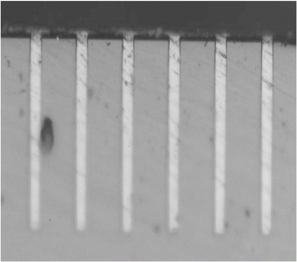
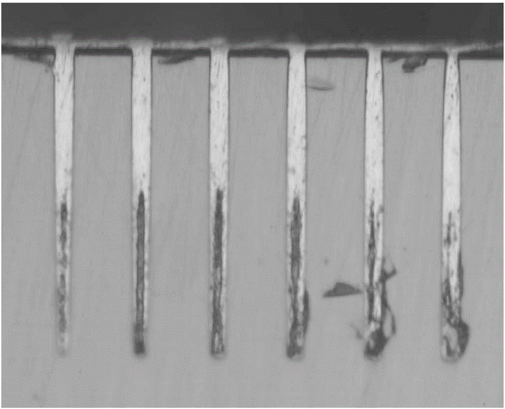
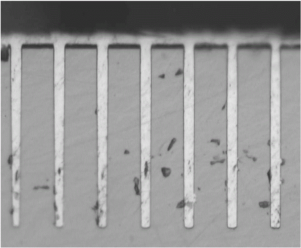
[0078] After copper plating to fill the TSVs, the wafer coupons were cross-sectioned and ima...
example 3
[0080] The method disclosed in Example 2 was repeated, but the inhibitor combination had the components in Table 4.
[0081] Table 4
[0082]
[0083] R is as defined in Example 1 above. The HLB of the triblock copolymer was determined to be 24 using the Davis method. The following table lists the variables used to calculate the HLB:
[0084] table 5
[0085] EO% lm w Mw PO #EO group #PO group #CH group # ether base #OH group 50 2300 2300 52 40 224 92 2
[0086] After filling the TSVs, they were analyzed by the same method as described in Example 2. No voids were observed in the sample. The cross-section of the sample looks similar to figure 1 Basically the same as shown in . All samples had a bright copper surface. There were no observable defects on the copper deposit.
PUM
| Property | Measurement | Unit |
|---|---|---|
| surface tension | aaaaa | aaaaa |
| surface tension | aaaaa | aaaaa |
| current density | aaaaa | aaaaa |
Abstract
Description
Claims
Application Information
 - R&D
- Intellectual Property
- Life Sciences
- Materials
- Tech Scout
- Unparalleled Data Quality
- Higher Quality Content
- 60% Fewer Hallucinations
Browse by: Latest US Patents, China's latest patents, Technical Efficacy Thesaurus, Application Domain, Technology Topic, Popular Technical Reports.
© 2025 PatSnap. All rights reserved.Legal|Privacy policy|Modern Slavery Act Transparency Statement|Sitemap|About US| Contact US: help@patsnap.com