Efficient blue-light quantum dot light emitting diode and preparation method therefor
A quantum dot light-emitting and diode technology, which is applied in semiconductor/solid-state device manufacturing, nanotechnology, electrical components, etc., can solve the problems of high difficulty and high cost, and achieve the effect of improving application life and increasing luminous efficiency
- Summary
- Abstract
- Description
- Claims
- Application Information
AI Technical Summary
Problems solved by technology
Method used
Image
Examples
Embodiment 1
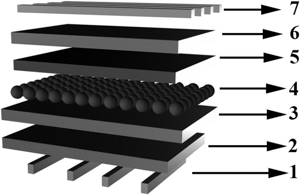
[0024] Blue quantum dot light-emitting diode devices, such as figure 1 As shown, it includes a cathode 1, an electron transport layer 2, a surface modification layer 3, a quantum dot light-emitting layer 4, a hole transport layer 5, a hole injection layer 6 and an anode electrode 7 formed on the substrate. The top is the electron transport layer, the surface modification layer, the quantum dot light-emitting layer, the hole transport layer, the hole injection layer and the anode. The electron transport layer can be composed of inorganic nanoparticles such as inorganic oxides or doped inorganic oxides. The surface modification layer can be composed of polymers containing simple aliphatic amine groups, including ethoxylated polyethyleneimine (PEIE), polyethyleneimine (PEI) and composite polymer materials composed of two polymers, to achieve the purpose of modifying the electron transport layer. The energy band structure is used to balance the injection of electrons and holes an...
Embodiment 2
[0034] Blue quantum dot light-emitting diode devices, such as figure 1 As shown, it includes a cathode 1, an electron transport layer 2, a surface modification layer 3, a quantum dot light-emitting layer 4, a hole transport layer 5, a hole injection layer 6 and an anode electrode 7 formed on the substrate. The top is the electron transport layer, the surface modification layer, the quantum dot luminescent layer, the hole transport layer, the hole injection layer and the anode. The electron transport layer is 40nm thick, the surface modification layer is 6nm thick, the quantum dot light emitting layer is 30nm thick, and the hole The thickness of the transport layer is 30nm, and the hole injection layer is 10nm. When the driving voltage of the quantum dot light-emitting diode device is greater than 3.3V, the luminous color remains stable, and the luminous color is blue; the luminous brightness is greater than 1000cd / m 2 , The device efficiency is greater than 3cd / A.
[0035] Th...
Embodiment 3
[0044] Blue quantum dot light-emitting diode devices, such as figure 1As shown, it includes a cathode 1, an electron transport layer 2, a surface modification layer 3, a quantum dot light-emitting layer 4, a hole transport layer 5, a hole injection layer 6 and an anode electrode 7 formed on the substrate. The top is the electron transport layer, the surface modification layer, the quantum dot luminescent layer, the hole transport layer, the hole injection layer and the anode. The electron transport layer is 50nm thick, the surface modification layer is 8nm thick, the quantum dot light emitting layer is 30nm thick, and the hole The thickness of the transport layer is 40nm, and the hole injection layer is 15nm. When the driving voltage of the quantum dot light-emitting diode device is greater than 3.3V, the luminous color remains stable, and the luminous color is blue; the luminous brightness is greater than 1000cd / m 2 , The device efficiency is greater than 3cd / A.
[0045] The...
PUM
 Abstract
Description
Claims
Application Information
 - Generate Ideas
- Intellectual Property
- Life Sciences
- Materials
- Tech Scout
- Unparalleled Data Quality
- Higher Quality Content
- 60% Fewer Hallucinations
Browse by: Latest US Patents, China's latest patents, Technical Efficacy Thesaurus, Application Domain, Technology Topic, Popular Technical Reports.
© 2025 PatSnap. All rights reserved.Legal|Privacy policy|Modern Slavery Act Transparency Statement|Sitemap|About US| Contact US: help@patsnap.com

