Serial-connection rolling based organic silicone resin light conversion body closely packaged LED processing method

A process method and organosilicon technology, applied in the direction of lamination devices, chemical instruments and methods, lamination, etc., can solve problems such as product consistency, thermal overstress, and yield reduction, so as to improve production efficiency and optimize production efficiency. The effect of improving product rate, improving light and color consistency, and improving product rate

Active Publication Date: 2017-03-01
JIANGSU CHERRITY OPTRONICS CO LTD
View PDF13 Cites 0 Cited by
  • Summary
  • Abstract
  • Description
  • Claims
  • Application Information

AI Technical Summary

Problems solved by technology

Although this method improves the uniformity of the coating thickness of the light conversion body through the screen printing process, and improves the uniformity of the phosphor particle distribution, so as to achieve the purpose of improving the yield; but there are still the following obvious deficiencies: one is that the screen printing The light converter of silicone resin is coated on the surface of the LED chip, and then due to the influence of thermal overstress during the baking and curing process, it will still cause local bubbles to form on the coating surface of the light converter coating and the LED chip to form unevenness The second is to fill the sealing mold or the lens cover with silica gel and package the LED chip coated with the light conversion body, and then the overall structure is baked and cured due to the influence of thermal overstress, which will still cause cracks in the sealing mold or lens cover. Bubbles are generated locally on the silicone surface layer to form uneven defects
The purpose of this method is to provide light converters uniformly arranged around the LED to prevent damage, so as to obtain an LED covered with a light converter layer and an LED device with the LED covered with a light converter layer; but there are also the following obvious Disadvantages: First, during the curing process of the fluorescent resin composition of the light conversion body, due to the influence of thermal overstress, it will still cause local bubbles to form on the surface layer of the light conversion body to form uneven defects; LEDs will still be affected by thermal overstress, resulting in a decrease in light efficiency during use of the LED; third, the process in the entire packaging process is relatively cumbersome, and the production efficiency of the packaged LED is not high; The displacement of the chip will inevitably lead to a decrease in the yield rate
Although the object of the invention of this proposal is to improve the uniformity of color and brightness, ease of manufacture, degree of freedom in design, etc. of the semiconductor light-emitting element to which the phosphor-containing resin layer is attached by the resin sheet laminate, but There are also the following obvious deficiencies: one is that the phosphor resin sheet used is a cured phosphor resin sheet, which will not be able to effectively eliminate possible residual pores, unevenness or other processing defects; the other is that in the bonding process, Pressing the pressure tool from the side of the semiconductor light-emitting element will damage the semiconductor light-emitting element; the third is to use the adhesive bonding process in the phosphor resin layer, which makes it difficult to remove the residue in the bonded semiconductor light-emitting element , the bonding process is very easy to produce pores, which will reduce the yield rate. At the same time, the existence of the adhesive layer also reduces the light extraction efficiency of the LED element; the fourth is the base of the phosphor resin sheet bonded to the light-emitting surface of the semiconductor light-emitting element. If the material is not peeled off, it will directly affect the light effect of the semiconductor light-emitting element; fifth, the phosphor resin layer is presented in a manner that multiple blocks are repeatedly arranged in rows in the length direction, but the realization of multiple blocks of the phosphor resin layer The configuration and the actual operation procedure are cumbersome, which will affect the packaging efficiency of the entire component. The location error of multiple blocks will directly affect the accuracy of subsequent bonding with the light-emitting components, and the size of multiple blocks In terms of thickness, if the consistency requirements cannot be met, it may cause serious product consistency problems

Method used


Image

  • Serial-connection rolling based organic silicone resin light conversion body closely packaged LED processing method
  • Serial-connection rolling based organic silicone resin light conversion body closely packaged LED processing method
  • Serial-connection rolling based organic silicone resin light conversion body closely packaged LED processing method

Examples


Embodiment 1

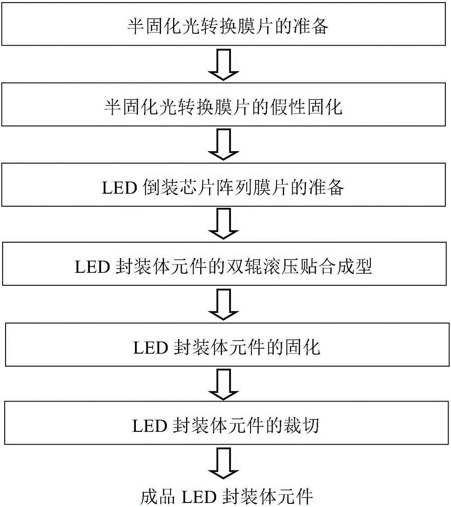
[0061] Example 1. combine figure 1 , the present invention proposes a process method based on series rolling of organic silicon resin light conversion body to package LED, which includes the preparation of semi-cured light conversion film, pseudo-curing of semi-cured light conversion film, LED flip-chip The preparation of the chip array diaphragm, the double-roller rolling lamination of the LED package components, the curing of the LED package components and the cutting process of the LED package components are a flow-type continuous process. The specific steps include the following:

[0062] Step 1, preparation of semi-cured light conversion film: obtain a semi-cured light conversion film composed of protective film A, semi-cured light conversion film and protective film B; the semi-cured light conversion film includes semi-cured silicone resin and light conversion material;

[0063] Step 2, Pseudo-curing of the semi-cured light-converting film: Under vacuum conditions, the...

Embodiment 2

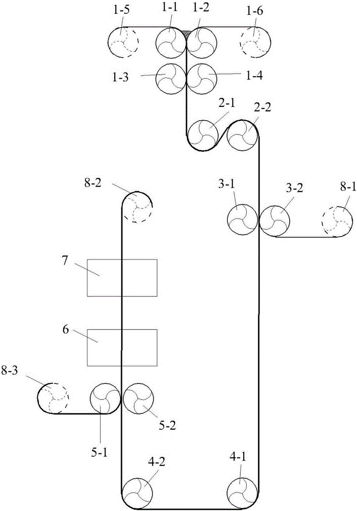
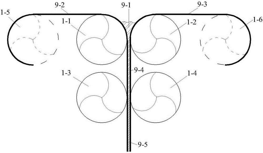
[0098] Example 2. The present invention proposes an equipment system based on the process method of tandem rolling organic silicon resin photo-converting body bonding and encapsulating LEDs. The film protective film peeling device adopts a light conversion film with a protective film on one side to package the LED flip chip array to form a rolling lamination device for LED package components; the protective film peeling device includes light conversion films that are connected in sequence Freezing part, traction and stripping of the one-side protective film after the photoconversion film is frozen, traction part and light conversion film reheating part; Roller.

[0099] The specific implementation scheme of the equipment system adopted by the process method of a series-rolled organic silicon resin light conversion body bonding and packaging LED proposed by the present invention is further disclosed as follows:

[0100] The light conversion film freezing component is a freezi...


PUM


Abstract

The invention relates to a serial-connection rolling based organic silicone resin light conversion body closely packaged LED processing method, comprising of the following continuous processes: the preparation of a half-solidified light conversion film, the false solidification of the half-solidified light conversion film, the preparation of an LED flip chip array film, the formation of an LED packaged element through double-roller rolling and attaching, solidifying the LED packaged element and the cutting of the LED packaged element. According to the invention, a continuous rolling technology is used to attach and package an LED, which meets the requirement to use an organic silicone resin light conversion body to attach and package an LED so as to raise the production efficiency and the qualified product rate of LED in industrialized LED packaging in batches.

Description

technical field [0001] The invention belongs to the technical field of light conversion body packaging LEDs, and in particular relates to a process method based on serial rolling of organic silicon resin light conversion body bonding packaging LEDs. Background technique [0002] LED has the advantages of high brightness, low heat, long life, environmental protection, renewable utilization, etc., and is called the most promising new generation of green lighting source in the 21st century. At present, although the theoretical life of LEDs can reach more than 100,000 hours, in actual use, due to the constraints of various factors such as chip failure, packaging failure, thermal overstress failure, electrical overstress failure or / and assembly failure, among them Package failure is particularly prominent, which makes LEDs prematurely experience light decay or light failure, which will hinder the progress of LEDs as a new type of energy-saving lighting source. In order to solve ...

Claims


Application Information

Patent Timeline
Patent Type & Authority Applications(China)
IPC IPC(8): H01L33/50H01L33/48H01L25/075
CPCH01L25/0753H01L33/48H01L33/505H01L2933/0041H01L2933/0033H01L33/501B32B37/0053B32B37/06B32B2037/1253B32B2457/00B32B37/08B32B2309/02B32B38/10H01L33/005H01L33/52H01L2933/005H01L33/56H01L25/075H01L33/50H01L27/153H01L33/483
Inventor 何锦华
Owner JIANGSU CHERRITY OPTRONICS CO LTD
Why Eureka
Try Eureka