A Package Structure of High Current Field Effect Transistor

A field effect tube and packaging structure technology, applied in the direction of circuits, electrical components, electric solid devices, etc., can solve the problems of affecting work, large volume, softening of solder joints, etc., and achieve the minimum overall structure, compact overall structure, and reliable connection Effect

Active Publication Date: 2018-10-26
中山市华星电源科技有限公司
View PDF3 Cites 1 Cited by
  • Summary
  • Abstract
  • Description
  • Claims
  • Application Information

AI Technical Summary

Problems solved by technology

[0003] The field effect tube packaging structure with the above structure, because the field effect tube has a high operating temperature and the heat dissipation effect is not good, it is easy to cause the solder joints to soften due to high temperature, resulting in poor contact between the field effect tube and the circuit board and affecting the work; in addition , using this packaging structure, its volume is large, which is not conducive to installation and use

Method used


Image

  • A Package Structure of High Current Field Effect Transistor
  • A Package Structure of High Current Field Effect Transistor
  • A Package Structure of High Current Field Effect Transistor

Examples


Embodiment Construction

[0031] Embodiments of the present invention will be described in detail below in conjunction with the accompanying drawings.

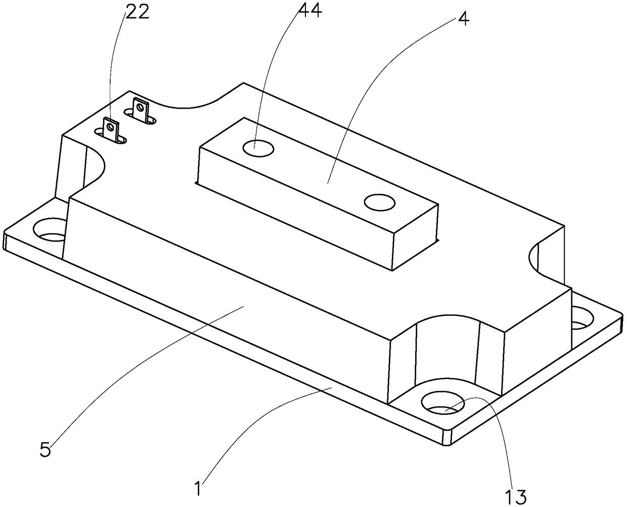
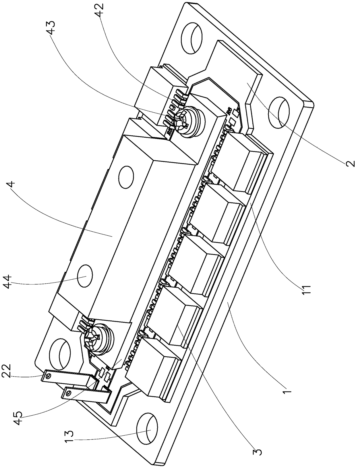
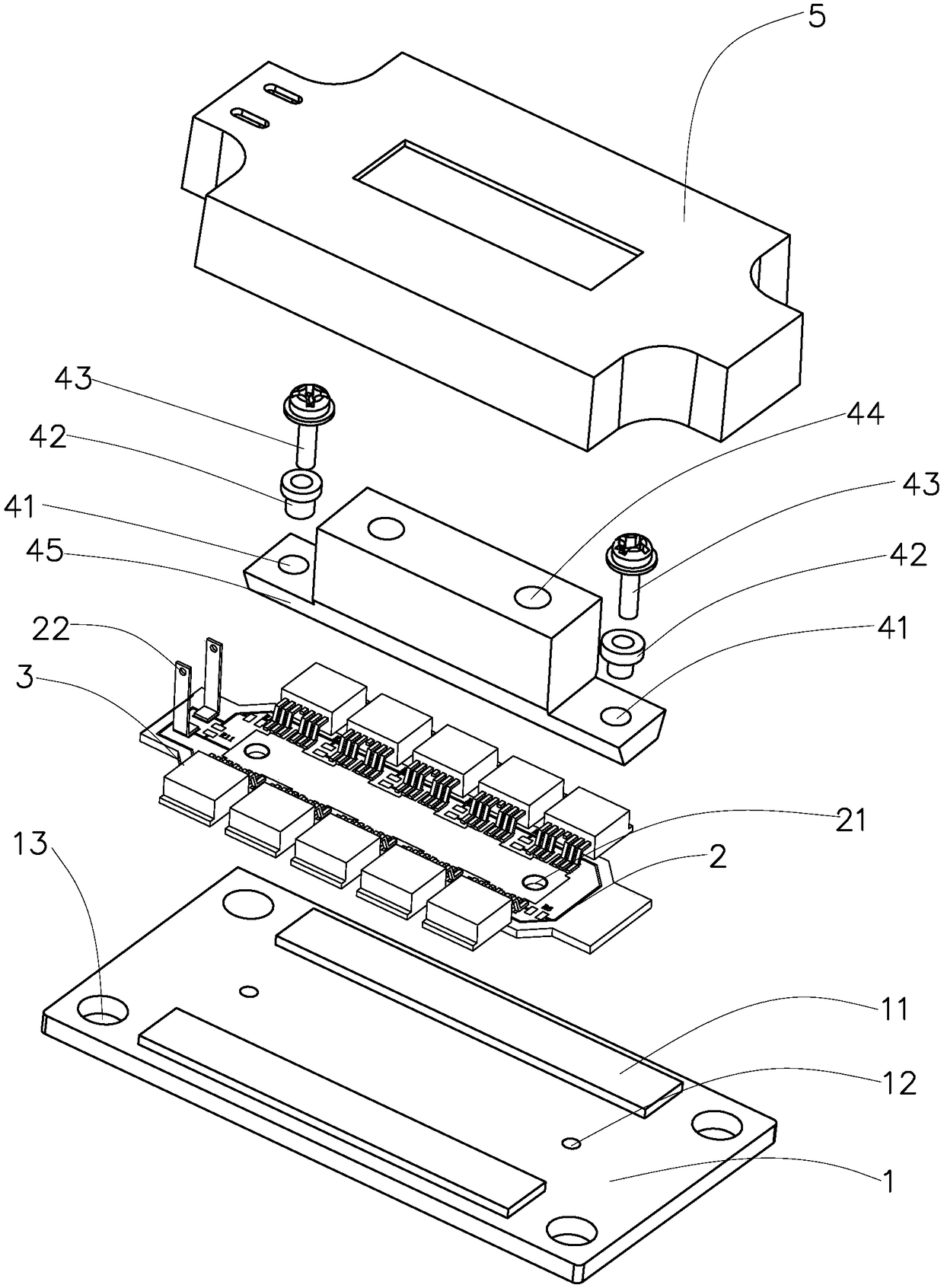
[0032] Such as figure 2 , image 3 and Figure 4 As shown, the packaging structure of a large current field effect transistor of the present invention includes a conductive base 1, an electrode connection base 4, a field effect tube 3 and a circuit board 2, and the electrode connection base 4 is fixedly insulated and connected to the conductive base 1 , and the circuit board 2 is placed between the electrode connection seat 4 and the conductive base 1, the bottom of the electrode connection seat 4 is electrically connected to the front of the circuit board 2, and the back of the circuit board 2 is connected to the conductive base 1, plural The G / S pole pins 31 of each of the field effect transistors 3 are all facing the electrode connection seat 4 and welded to the side of the circuit board 2, and the D pole pins 32 of each of the field effect trans...


PUM


Abstract

The invention discloses a packaging structure of heavy current field effect transistors. A conductive base capable of realizing electrical conduction and heat radiation is employed, a bottom surface of a circuit board is fixed on the conductive base, a bottom portion of an electrode connection seat is in conductive connection with a front side of the circuit board, G / S electrode pins of the field effect transistors face towards the electrode connection seat and are welded with the circuit board, and D-electrode pins of the field effect transistors face outside and are in conductive connection with the conductive base so as to realize parallel arrangement of all the field effect transistors. The packaging structure is advantaged in that properties of compact structure, small volume, reliable connection and low cost are realized, the D-electrode pins of all the field effect transistors are conductively welded on the conductive base so as to realize excellent heat radiation, after all the field effect transistors are connected in parallel, output currents are gathered and outputted through the electrode connection seat, and the packaging structure can effectively adapt to heavy-current and large-power work environments.

Description

【Technical field】 [0001] The invention relates to a packaging structure of electronic components, in particular to a packaging structure of a large current field effect transistor. 【Background technique】 [0002] Field effect tubes are widely used in the industrial fields of synchronous rectification switching power supply and pulse power supply. For this reason, many packaging structures of field effect tubes are involved in the prior art. Generally, the package structure of high current is to directly weld the field effect tubes on the circuit board. Then fix the circuit board on the corresponding conductive base, and finally carry out the corresponding packaging. [0003] The field effect tube packaging structure with the above structure, because the field effect tube has a high working temperature and the heat dissipation effect is not good, it is easy to cause the solder joints to soften due to high temperature, resulting in poor contact between the field effect tube an...

Claims


Application Information

Patent Timeline
Patent Type & Authority Patents(China)
IPC IPC(8): H01L23/495H01L23/24H01L25/07
Inventor 邓勇将欧扣锋卢桦岗
Owner 中山市华星电源科技有限公司
Why Eureka
Try Eureka