Electron transport material for organic electroluminescence device

A technology for electron transport materials and electroluminescent devices, which is applied in the field of cross-linkable electron transport materials, can solve the problems of improving and destroying the lower organic functional layer, and the surface roughness of the lower organic functional layer becomes larger, so as to improve the mobility , easy synthesis, and good hole-blocking properties

Active Publication Date: 2017-02-22
SUZHOU INST OF NANO TECH & NANO BIONICS CHINESE ACEDEMY OF SCI
View PDF4 Cites 11 Cited by
  • Summary
  • Abstract
  • Description
  • Claims
  • Application Information

AI Technical Summary

Problems solved by technology

When the solution method is used for processing, the solution in the upper layer will erode the lower organic functional layer, causing the surface roughness of the lower organic functional layer to increase, or even directly destroying the lower organic functional layer.
The contact problem of the functional layer interface caused by the defects on the surface morphology will seriously affect the efficiency and life of the device, which is not conducive to the improvement of the performance of the OLED device.

Method used


Image

  • Electron transport material for organic electroluminescence device
  • Electron transport material for organic electroluminescence device
  • Electron transport material for organic electroluminescence device

Examples


example 1

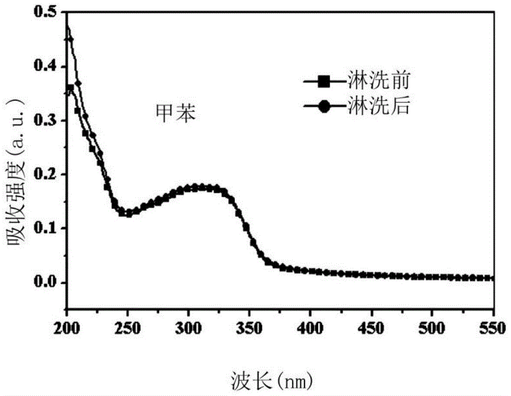
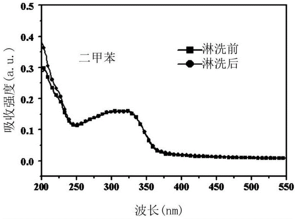
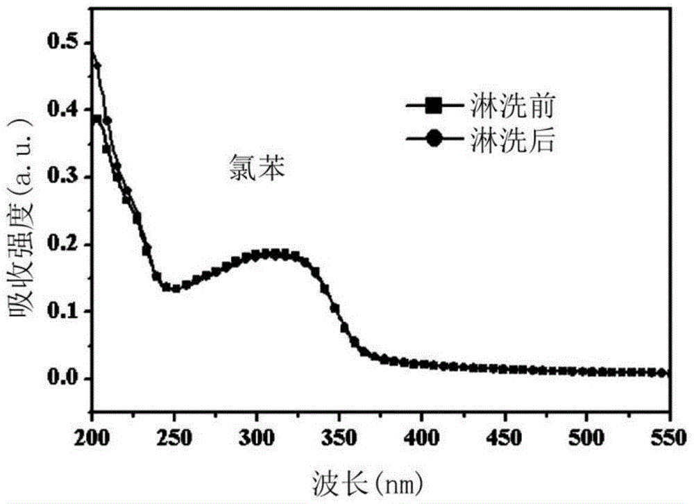
[0145] Evaluation Example 1: Study on the Anti-solvent Erosion Properties of Compounds 1, 4, 7, 10 and 13

[0146] Figure 1 to Figure 4 Graphs showing absorption spectra of an electron transport material (Compound 1) for organic electroluminescent devices according to an exemplary embodiment of the present invention before and after rinsing with toluene, xylene, chlorobenzene and methylene chloride, respectively. Figure 5 to Figure 8 Graphs showing absorption spectra of an electron transport material (compound 4) for organic electroluminescent devices according to an exemplary embodiment of the present invention before and after rinsing with toluene, xylene, chlorobenzene and methylene chloride, respectively. Figure 9 to Figure 12 Graphs showing absorption spectra of an electron transport material (compound 7) for organic electroluminescent devices according to an exemplary embodiment of the present invention before and after rinsing with toluene, xylene, chlorobenzene and...

example 2

[0150] Evaluation Example 2: Organic Light Emitting Diode Device

[0151] Figure 21 A schematic cross-sectional view showing an organic light emitting diode device formed using an electron transport material for an organic electroluminescent device according to an exemplary embodiment of the present invention. Figure 22 to Figure 23 A current density-voltage-brightness graph and a voltage-efficiency graph of an organic light emitting diode device formed using the electron transport material (compound 1) for an organic electroluminescent device according to an exemplary embodiment of the present invention are shown, respectively. Figure 24 to Figure 25 A current density-voltage-brightness graph and a voltage-efficiency graph of an organic light emitting diode device formed using the electron transport material (compound 1) for an organic electroluminescent device according to an exemplary embodiment of the present invention are shown, respectively. Figure 26 An electrolu...


PUM

PropertyMeasurementUnit
current efficiencyaaaaaaaaaa

Abstract

The invention provides an electron transport material for an organic electroluminescence device. The electron transport material comprises a compound expressed by a formula A-C-A or a formula as shown in the description; a group A is expressed by a following formula 1 as shown in the description; definitions of R1, R2, R3 and a crosslinked group C are just as defined in the description. Compared with a traditional host material, the electron transport material for the organic electroluminescence device, provided by the exemplary embodiment of the invention, can be easily prepared through a solution method, has a favorable anti-solvent-erosion ability, and has the characteristics of easiness in synthesis and purification of small molecule materials, and network polymers formed after cross-linking and solidification can be beneficial to remarkably improving the electron mobility.

Description

technical field [0001] The invention belongs to the technical field of chemical synthesis, and in particular relates to a cross-linkable electron-transporting material used in solution processing to prepare organic electroluminescent devices. Background technique [0002] Organic Light-emitting Diode (OLED) is an electroluminescent device based on organic semiconductor materials. There are mainly two manufacturing processes, namely, vacuum evaporation method and solution processing method. In the field of organic full-color display, domestic and foreign companies basically use vacuum evaporation and printing technology to prepare display screens, which is the current international mainstream development technology. The vacuum evaporation technology of small molecules has matured relatively early, and has now achieved industrialization, and full-color displays of various sizes have been applied to electronic devices such as smart watches, mobile phones, tablet computers, and ...

Claims


Application Information

Patent Timeline
Patent Type & Authority Applications(China)
IPC IPC(8): C09K11/06C07D249/08C07D401/14C07D403/14C07D413/14C07D405/14C07D409/14C07D471/06C07F7/10H01L51/54
Inventor 庄锦勇魏昌庭苏文明崔铮
Owner SUZHOU INST OF NANO TECH & NANO BIONICS CHINESE ACEDEMY OF SCI
Why Eureka
Try Eureka