Device and method for pinhole alignment of point diffraction interferometer
A point-diffraction interferometer and pinhole technology, which is applied in the field of devices for point-diffraction interferometer pinhole alignment, can solve the problems of long time-consuming and high cost for precise alignment of the point-diffraction interferometer pinhole, and achieves short time-consuming, high precision effect
- Summary
- Abstract
- Description
- Claims
- Application Information
AI Technical Summary
Problems solved by technology
Method used
Image
Examples
Embodiment 1
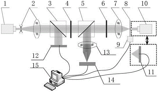
[0048] Such as figure 1 Shown is a schematic structural diagram of the pinhole alignment device used in the point-diffraction interferometer in Embodiment 1. The device includes a first laser 1, a laser beam expander 2, a first dichroic prism 3, a half-wave plate 4, a second dichroic prism 5, a quarter-wave plate 6, a focusing mirror 7, and a pinhole plate 8 , a three-dimensional adjustment mechanism 9, a second laser 10, a second laser power meter 11, a first laser power meter 12, a rear group lens 13 for imaging, a CMOS camera 14, and a computer 15.
[0049] In this embodiment, the working principle of the pinhole alignment device for the point diffraction interferometer is as follows:
[0050] The first laser 1 is used to emit linearly polarized laser light. The laser beam expander 2 expands and collimates the linearly polarized laser light. The splitting ratio of the first dichroic prism 3 makes most of the laser light transmit and a small part of the laser light is refle...
Embodiment 2
[0061] This embodiment provides a method for realizing pinhole micron level coarse alignment:
[0062] S1.1, first turn on the second laser 10, the laser beam directly illuminates and passes through the pinhole on the pinhole plate 8, at this time, the illumination spot is large, and the pinhole can be easily illuminated, and the laser beam passes through the focusing mirror 7, four Arrive at the CMOS camera 14 after the one-third wave plate 6, the second dichroic prism 5 and the rear group lens 13 for imaging, observe the first light spot O1 that can be seen on the CMOS camera 14, and record the position of the light spot O1 as P1;
[0063] S1.2. Turn on the first laser 1, and the emitted laser light passes through the laser beam expander 2, the first dichroic prism 3, the half-wave plate 4, the second dichroic prism 5, the quarter-wave plate 6 and the focusing The mirror 7 converges and illuminates on the pinhole plate 8, and the light beam reflected by the pinhole plate 8 ...
Embodiment 3
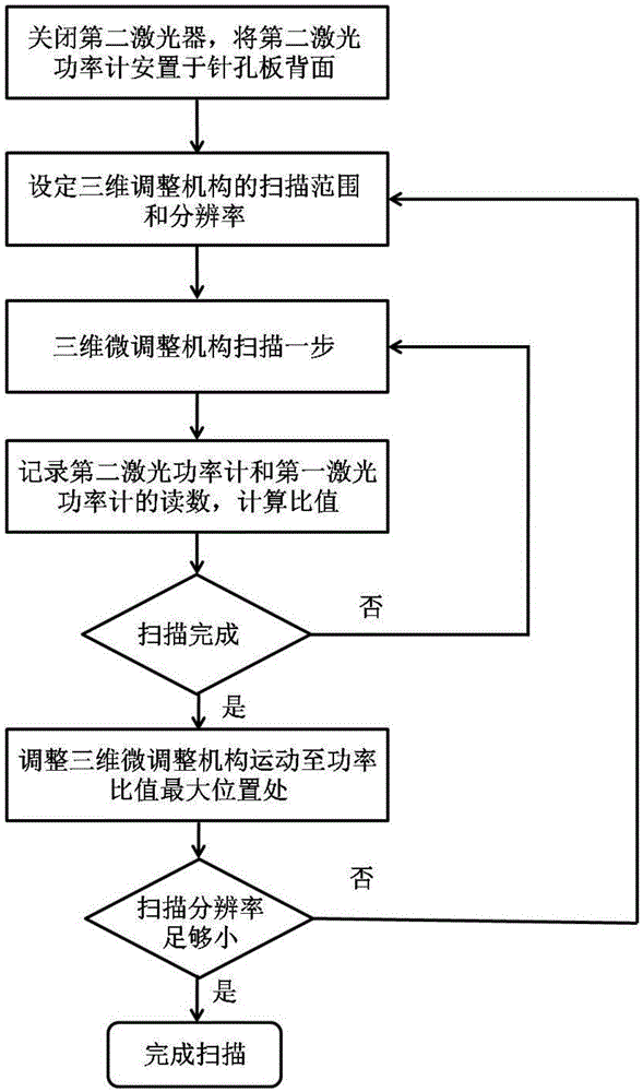
[0066] Such as figure 2 As shown, the flow chart for realizing pinhole precision alignment provided by this embodiment:
[0067] S2.1. Turn off the second laser 10, place the second laser power meter 11 behind the pinhole plate 8, and detect the power of the pinhole diffracted light;
[0068] S2.2. Set the scanning range of the three-dimensional adjustment mechanism 9 to be 10 μm×10 μm, the scanning resolution to be 1 μm, and the total number of scanning points to be 100;
[0069] S2.3. Control the three-dimensional adjustment mechanism 9 to scan one step in a two-dimensional plane of 10 μm×10 μm;
[0070] S2.4. Record the measured values and ratios of the second laser power meter 11 and the first laser power meter 12 for each scanning step;
[0071] S2.5. Determine whether the scanning of the three-dimensional adjustment mechanism 9 is completed. If not, repeat steps 2.3-2.4. If it is completed, proceed to the next step 2.6. Steps 2.3-2.4 need to be repeated 100 times th...
PUM
 Abstract
Description
Claims
Application Information
 - R&D Engineer
- R&D Manager
- IP Professional
- Industry Leading Data Capabilities
- Powerful AI technology
- Patent DNA Extraction
Browse by: Latest US Patents, China's latest patents, Technical Efficacy Thesaurus, Application Domain, Technology Topic, Popular Technical Reports.
© 2024 PatSnap. All rights reserved.Legal|Privacy policy|Modern Slavery Act Transparency Statement|Sitemap|About US| Contact US: help@patsnap.com


