
High-density integration tile-type active phased-array antenna structure

A phased array antenna, high-density technology, applied in the connection of antenna grounding switch structure, antenna, antenna array, etc., can solve the problem of increasing the weight, volume and cost of the final antenna, the difficulty of assembly and production of the antenna, and a large number of connectors, etc. problem, to achieve the effect of easy product quality control, shortened processing cycle and obvious cost

Active Publication Date: 2016-12-07
10TH RES INST OF CETC
View PDF3 Cites 39 Cited by
  • Summary
  • Abstract
  • Description
  • Claims
  • Application Information

AI Technical Summary

Problems solved by technology

These modules still need to be interconnected by radio frequency and low frequency through various connectors. A large number of connectors are required, which is costly. In addition, during the installation process, it is necessary to consider such issues as how to install in position, the insertion and withdrawal force of connectors, etc.
Such an architecture design will undoubtedly increase the weight, volume and cost of the final antenna
In addition, due to the large number of components and parts involved, it is difficult to assemble and produce the complete antenna, so the natural efficiency and yield will not be too high, and the cost will increase accordingly

Method used


Image

  • High-density integration tile-type active phased-array antenna structure

Examples


Embodiment Construction

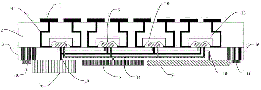
[0014] refer to figure 1 . figure 1 A best implementation example of a high-density integrated integrated tile-type active phased array antenna architecture of the present invention is described. The high-density integrated integrated tile-type active phased array antenna architecture includes a basic tile layer, and the basic tile layer includes: a cooling layer, a DC power supply and control circuit layer, an RF feeding layer, and a radiation element layer. It is mainly composed of the metal radiation patch 1, the upper multi-layer PCB board 2, and the lower multi-layer printed board on the upper multi-layer PCB board 2 and the lower multi-layer PCB board 3 based on PCB high-density integration. Board 3, MMIC chip 5, channel component 7, power supply component 8, and beam control component 9. For the upper multilayer PCB board 2, the metal radiation patch 1, the radio frequency feeder 4 and the metal shielding cavity contained therein are all realized by using multilayer P...


PUM


Abstract

The invention discloses a high-density integration tile-type active phased-array antenna structure, and aims to provide a high-integration tile-type active phased-array antenna structure which is smaller in volume, lighter in weight, lower in cost and stable in performance and can eliminate a self-excitation phenomena. The structure is realized through the following technical scheme: a radiation array element layer is arranged on an upper multi-layer PCB (2), each metal radiation patch (1) array module is electrically connected to an MMIC chip (5) through a radio-frequency feeder line (4), the MMIC chips are packaged in metal sealed cavities (12) between the upper multi-layer PCB and a lower multi-layer PCB to form the RF feeder layer; each MMIC chip is electrically connected to a channel assembly (7), a power supply assembly (8) and a beam control assembly (9) which are positioned on the lower bottom plane of a multi-layer printed board (3) respectively, and an DC power supply and a control circuit layer are formed by the MMIC chips as well as a radio-frequency external interface (10) and a control and power supply external interface (11) which are arranged at two ends of the bottom of the multi-layer printed board respectively.

Description

technical field [0001] The invention relates to a tile-type active phased array antenna structure widely used in the fields of communication, navigation, identification, measurement and control, early warning detection, precision tracking, broadcasting and television, remote sensing and telemetry, and radio astronomy. Background technique [0002] The phased array antenna is the core part of the phased array system, especially the two-dimensional active phased array antenna, whose integration level determines the performance and cost of the entire system. Although the cost of an active phased array antenna is not the primary factor, the volume, weight and power consumption requirements are very stringent. Active phased array antennas can be roughly divided into brick type and tile type according to the circuit assembly method. The brick-type active phased array antenna can be considered as the first generation product, which has the disadvantages of heavy weight, bulky volu...

Claims


Application Information

Patent Timeline
IPC IPC(8): H01Q21/00H01Q23/00H01Q1/50H01Q1/02
CPCH01Q1/02H01Q1/50H01Q21/00H01Q23/00H01Q1/2283H01Q21/065H01Q3/34
Inventor 张剑周太富蓝海张云何海丹
Owner 10TH RES INST OF CETC
Learn More