NAND gate flash memory and its operation method

A non-gate flash and memory technology, applied in the field of NAND flash memory array architecture, can solve problems such as long read delay time and limitation, achieve low power consumption, reduce read delay, and avoid accidental programming and the effect of programming interference

Active Publication Date: 2018-03-30
WINBOND ELECTRONICS CORP
View PDF9 Cites 0 Cited by
  • Summary
  • Abstract
  • Description
  • Claims
  • Application Information

AI Technical Summary

Problems solved by technology

Unfortunately, because NAND flash memory often has a long read latency (read latency time), the NAND flash memory is limited in applications that require random access and continuous page reading

Method used


Image

  • NAND gate flash memory and its operation method
  • NAND gate flash memory and its operation method
  • NAND gate flash memory and its operation method

Examples


Embodiment Construction

[0051] The illustrated embodiments or examples of the invention will be described as follows. The scope of the present invention is not limited thereto. Those skilled in the art should be able to understand that some modifications, substitutions and substitutions can be made without departing from the spirit and structure of the present invention. In the embodiments of the present invention, element symbols may be used repeatedly, and several embodiments of the present invention may share the same element symbols, but the characteristic elements used in one embodiment are not necessarily used in another embodiment.

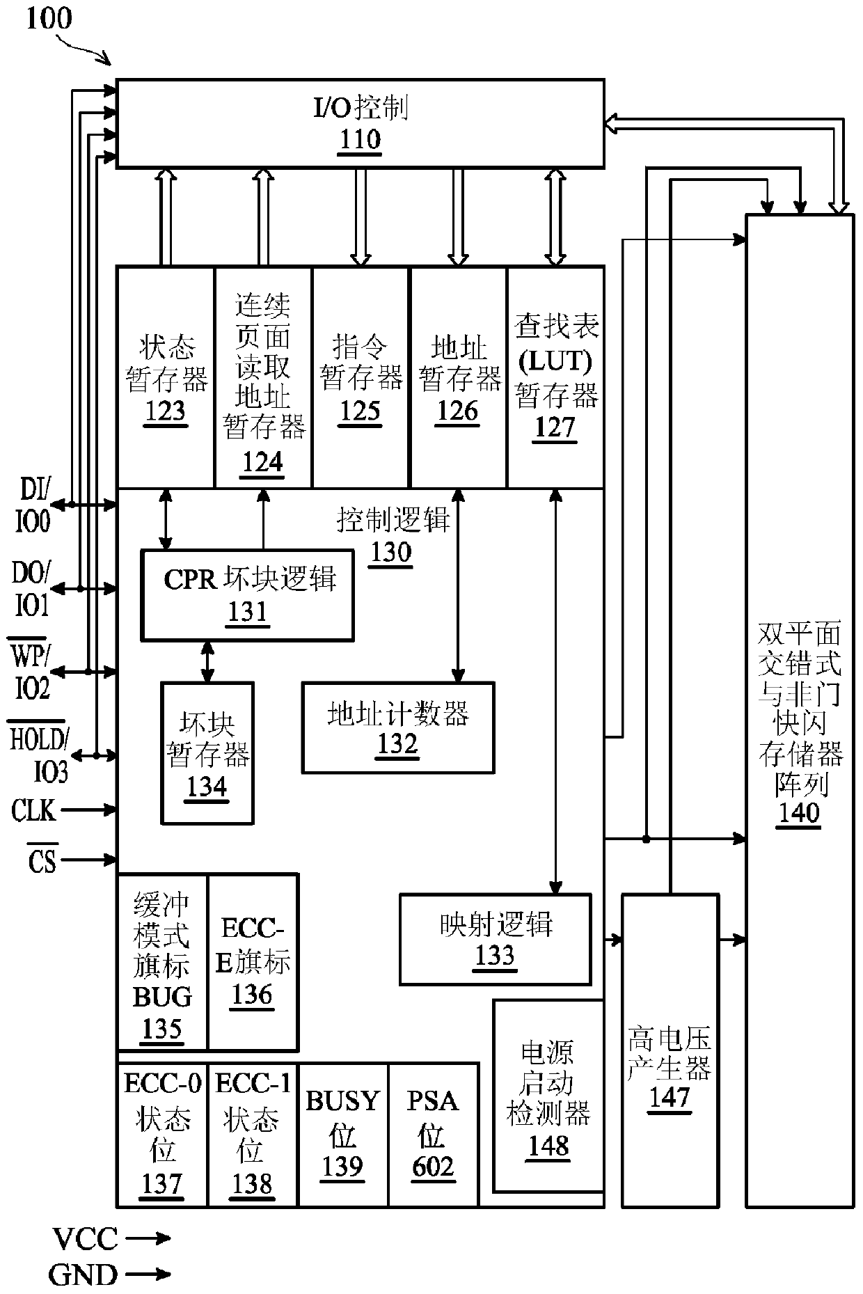
[0052] In order to compete with NOR flash memory devices in specific applications, NAND flash memory devices should have the following characteristics, including: (1) Multiple input / output serial peripheral interface (SPI) or multiple input / output quad Peripheral interface (Quad Peripheral Interface, QPI); (2) Small size and low pin count package type (density as...


PUM


Abstract

The present invention provides a kind of NAND gate flash memory and its operation method, and this NAND gate flash memory comprises: an input / output bus bar; The planes are configured to be alternately coupled to the input / output bus bars. The invention can reduce the reading delay and avoid accidental programming and programming interference, and the corresponding NOR flash memory can keep the higher memory density and low power consumption characteristics of the traditional NAND flash memory. Reduced read latency is achieved by using smaller series of NAND gates to avoid reduced read current. Each memory plane in an interleaved dual-plane memory structure is relatively small thus using word lines with lower RC delay and bit lines to achieve a reverse-biasing mechanism for uninterrupted reading of different pages and blocks and avoiding accidental programming and program disturb.

Description

technical field [0001] The present invention relates to digital memory devices and their operations, and more particularly to NAND flash memory array architectures with low read latency and low program disturbance. Background technique [0002] NAND flash memory is often used for data storage. In a density above 512 Mbits, the cost of a single level cell (Single Level Cell, “SLC”) NAND flash memory has a great advantage. This is due to the smaller size memory cells used in SLC-NAND flash memory itself. [0003] With the development of various technologies suitable for NAND flash memory, NAND flash memory is also often used in various applications other than data storage. Unfortunately, because the NAND flash memory often has a long read latency (read latency), the NAND flash memory is limited in applications that require random access and continuous page reading. Contents of the invention [0004] The present invention provides a NAND gate flash memory and its operation...

Claims


Application Information

Patent Timeline
Patent Type & Authority Patents(China)
IPC IPC(8): G11C16/06G11C16/26
CPCG11C7/18G11C8/12G11C16/26G11C16/0483G11C16/08G11C16/10
Inventor 李钟午安尼尔·古普特金大铉
Owner WINBOND ELECTRONICS CORP
Why Eureka
Try Eureka