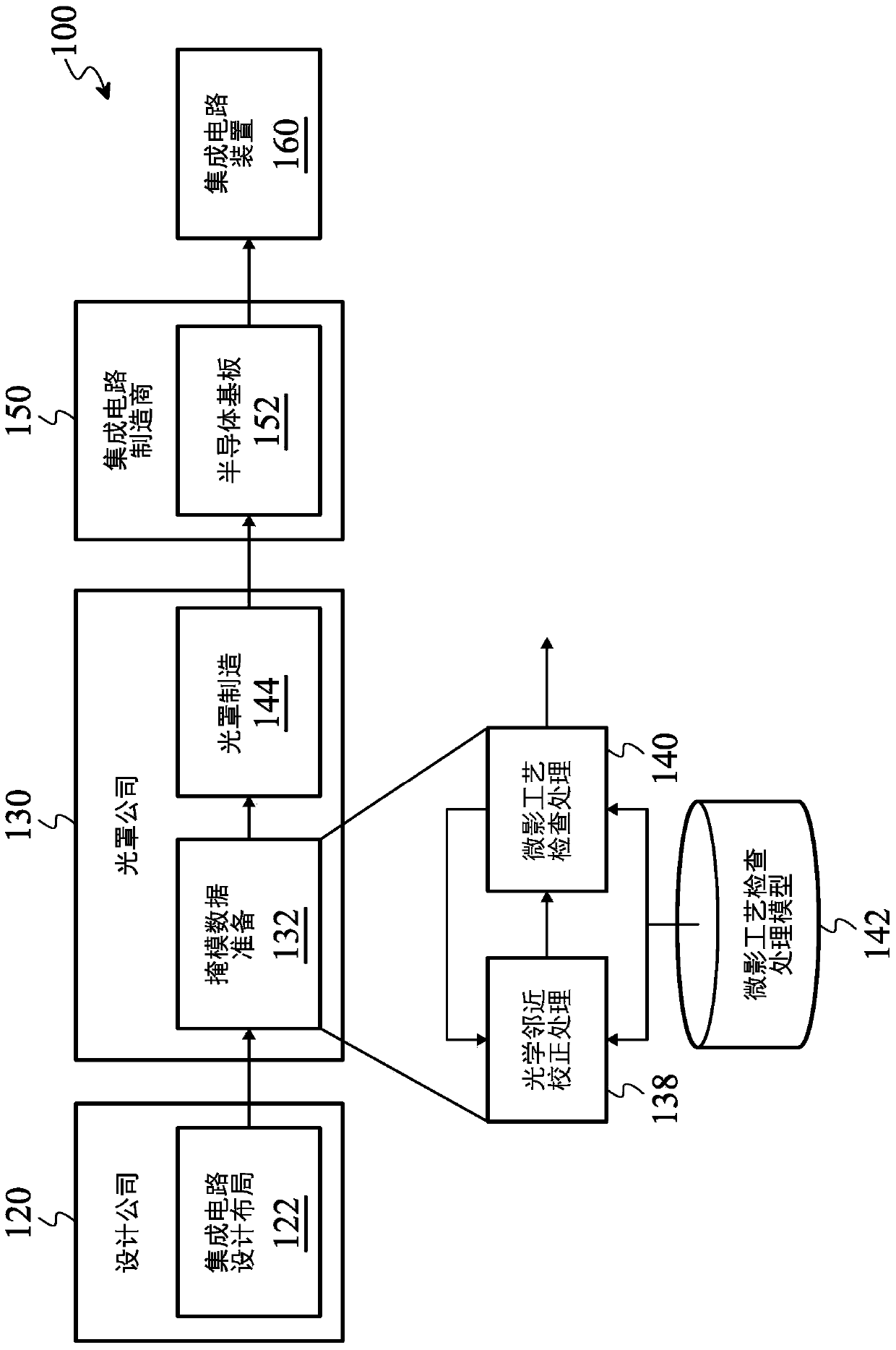
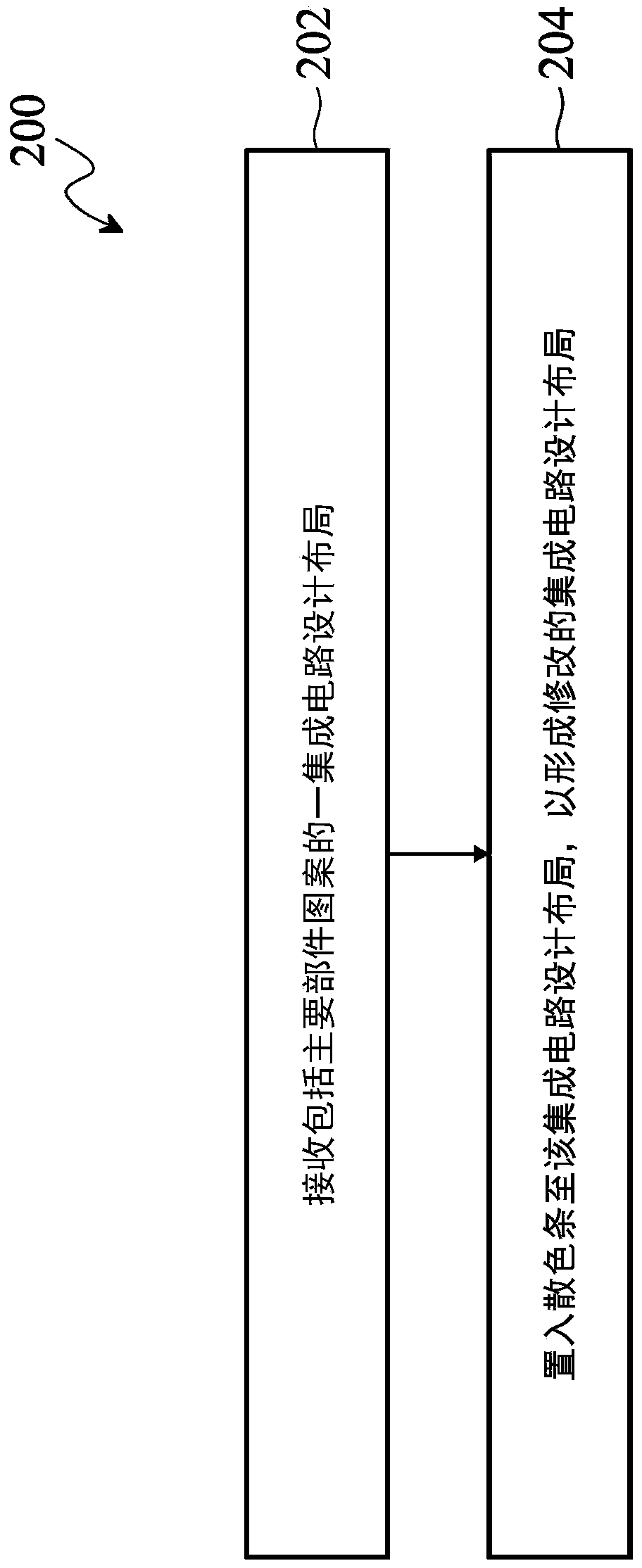
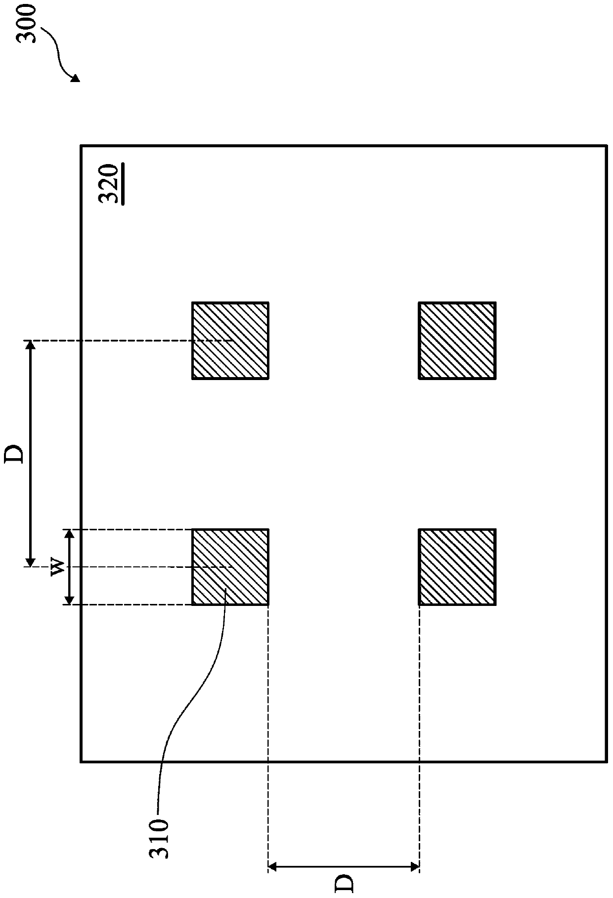
The Method of Incorporating Scattering Strips into the Lithography Process
A color bar and placement technology, which is applied in the field of lithography using dispersive color bars, can solve the problems of increasing the processing complexity of integrated circuits, and achieve the effects of improving the depth of focus and reducing the printing window.
- Summary
- Abstract
- Description
- Claims
- Application Information
AI Technical Summary
Problems solved by technology
Method used
Image

Examples
Embodiment Construction
[0056] The following disclosure provides many different embodiments, or examples, for implementing different features of the invention. Specific embodiments of components and arrangements will be described below to make the disclosure of the present invention clearer and easier to understand. The embodiments listed here should only be examples, and are not intended to limit the present invention. For example, a description of a first feature by or on a second feature may include an embodiment in which the first and second features are formed by direct contact, and may also include an embodiment in which the first and second features may be formed in direct contact. In an embodiment where additional features are formed between, the first and second features in this case may not be formed by direct contact. In addition, the reference numerals and / or letters disclosed in the present invention may appear repeatedly in different embodiments. The purpose of the repeated description...
PUM
 Abstract
Description
Claims
Application Information
 - R&D
- Intellectual Property
- Life Sciences
- Materials
- Tech Scout
- Unparalleled Data Quality
- Higher Quality Content
- 60% Fewer Hallucinations
Browse by: Latest US Patents, China's latest patents, Technical Efficacy Thesaurus, Application Domain, Technology Topic, Popular Technical Reports.
© 2025 PatSnap. All rights reserved.Legal|Privacy policy|Modern Slavery Act Transparency Statement|Sitemap|About US| Contact US: help@patsnap.com