
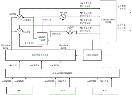
Method and system for realizing ultrahigh-speed digital orthogonal down conversion and decimation filtering in FPGA

A technology of digital quadrature and decimation filtering, which is applied in transmission systems, digital technology networks, impedance networks, etc., can solve problems such as difficult design, achieve the effects of shortening the development cycle, improving scalability, and stably receiving and processing data

Inactive Publication Date: 2016-08-31
XINYANG NORMAL UNIVERSITY
View PDF2 Cites 22 Cited by
  • Summary
  • Abstract
  • Description
  • Claims
  • Application Information

AI Technical Summary

Problems solved by technology

[0004] The technical problem to be solved by the present invention is to provide a method and system for realizing ultra-high-speed digital quadrature down-conversion and decimation filtering in FPGA. The present invention solves the problem of using FPGA to receive ADC data and perform quadrature Difficult technical problems in the design of down-conversion

Method used


Image

  • Method and system for realizing ultrahigh-speed digital orthogonal down conversion and decimation filtering in FPGA
  • Method and system for realizing ultrahigh-speed digital orthogonal down conversion and decimation filtering in FPGA
  • Method and system for realizing ultrahigh-speed digital orthogonal down conversion and decimation filtering in FPGA

Examples


Embodiment Construction

[0045] 1) AD device selection strategy

[0046] At present, there are three main types of external output data interfaces of high-speed AD conversion devices (Analog–to-Digital Converter hereinafter referred to as ADC): parallel LVTTL single-ended level output; serial LVDS differential level; and parallel LVDS differential level. Among these three types, LVTTL single-ended level is generally only used in occasions where the frequency does not exceed 100MHz due to its push-pull output architecture. This interface is rarely seen in ultra-high-speed AD devices. Typical products such as Linear Technology The LTC2208; the serial LVDS differential level only uses a pair of high-speed LVDS differential ports to complete data transmission, which greatly reduces the data port occupation. It is often used in single-chip multi-channel AD devices. The typical product is AD9259 from Analog Devices. However, when When the ADC sampling frequency is high, the operating frequency of serial LVD...


PUM


Abstract

The invention discloses a method and a system for realizing ultrahigh-speed digital orthogonal down conversion and decimation filtering in an FPGA. The system comprises the components of a plurality of ADC sampling chips, a high-speed ADC data receiving module, an over-clock processing module, a global clock module, a local numerical control oscillator and a multichannel digital decimation filter. The designed working frequency of the traditional FPGA is hard to exceed 200MHz. According to the method and the system, a numerical control oscillator (NCO) and the digital decimation filter as core parts in orthogonal down conversion are improved; furthermore through reasonably restraining layout and wiring of the FPGA, highest sampling rate above 500Msps and output baseband data rate above 125MHz can be ensured on a common FPGA device. Furthermore the method and the device can support simultaneous parallel sampling of multiple paths of ADC data, thereby adapting with a multichannel data receiving occasion.

Description

technical field [0001] The invention relates to the field of digital communication and radar signal processing, in particular to a method and system for realizing ultra-high-speed digital quadrature down-conversion and extraction filtering in FPGA. Background technique [0002] FPGA is the English abbreviation of Field Programmable Gate Array (Field Programmable Gate Array), which contains a large number of programmable resources, including look-up tables LUTs, registers, memories, hardware multipliers, phase-locked loops, etc. The programmable resources inside the FPGA chip can work in parallel, so it has extremely powerful processing capabilities, and its computing capabilities can reach hundreds of times or even higher than that of traditional CPUs. It is precisely because of this that in many signal processing platforms, FPGA assumes the core functions of computing and scheduling, and its main development method relies on hardware description language (hereinafter referr...

Claims


Application Information

Patent Timeline
IPC IPC(8): H04B1/18H03H17/00
CPCH03H17/00H03H2017/0081H04B1/18
Inventor 王鹏龚克涂友超徐涛康鑫向磊连帅彬余大庆
Owner XINYANG NORMAL UNIVERSITY
Learn More