Full back electrode contact crystalline silicon solar cell structure and preparation method thereof

A full-back electrode contact and solar cell technology, applied in the field of solar cells, can solve the problems of high material cost, recombination loss, and resistance loss, etc., and achieve the effects of reducing the amount of silver electrodes used, reducing recombination loss, and improving conversion efficiency

Active Publication Date: 2018-07-17
LONGI SOLAR TECH (TAIZHOU) CO LTD
View PDF6 Cites 0 Cited by
  • Summary
  • Abstract
  • Description
  • Claims
  • Application Information

AI Technical Summary

Problems solved by technology

At present, the electrodes of crystalline silicon solar cells are mostly screen-printed with silver paste to form nearly a hundred fine grids and several main grids. The materials used in this process are expensive, and the silver electrodes will cause 5% to 7% of the surface of the cell. The area forms the shading of light, resulting in resistive loss and recombination loss at the same time
[0004] The back contact battery solves the light shielding problem of the metal grid wire because the metal electrode of the battery is wound back to the back of the battery, but the amount of silver or other conductive metals in the electrode has not been reduced, on the contrary, it is slightly higher than that of conventional batteries. Increase

Method used


Image

  • Full back electrode contact crystalline silicon solar cell structure and preparation method thereof
  • Full back electrode contact crystalline silicon solar cell structure and preparation method thereof
  • Full back electrode contact crystalline silicon solar cell structure and preparation method thereof

Examples


Embodiment 1

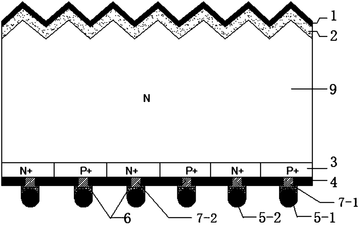
[0055] (1) The N-type monocrystalline silicon wafer is anisotropically etched in a KOH solution at about 80°C to obtain a pyramid structure on the surface.

[0056] (2) Print a boron-containing interdigitated diffusion mask layer on the back of the silicon wafer, and then perform phosphorus-doped thermal diffusion at about 750-850°C. The boron on the mask layer enters the silicon substrate after diffusion to form a P-type The doped layer, and the area where the mask layer is not printed, forms an N-type doped layer after phosphorus is diffused. The width of a single P-type doped strip region on the back is 500um, and the square resistance is 70Ω / □; the width of a single N-type doped strip region on the back is 300um, and the square resistance is 70Ω / □. This process simultaneously forms a 100Ω / □ N+ doped layer on the front side of the silicon wafer.

[0057] (3) The phosphosilicate glass and borosilicate glass on the front and back are removed by wet etching.

[0058] (4) Dep...

Embodiment 2

[0066] (1) The N-type monocrystalline silicon wafer is anisotropically etched in a KOH solution at about 80°C to obtain a pyramid structure on the surface.

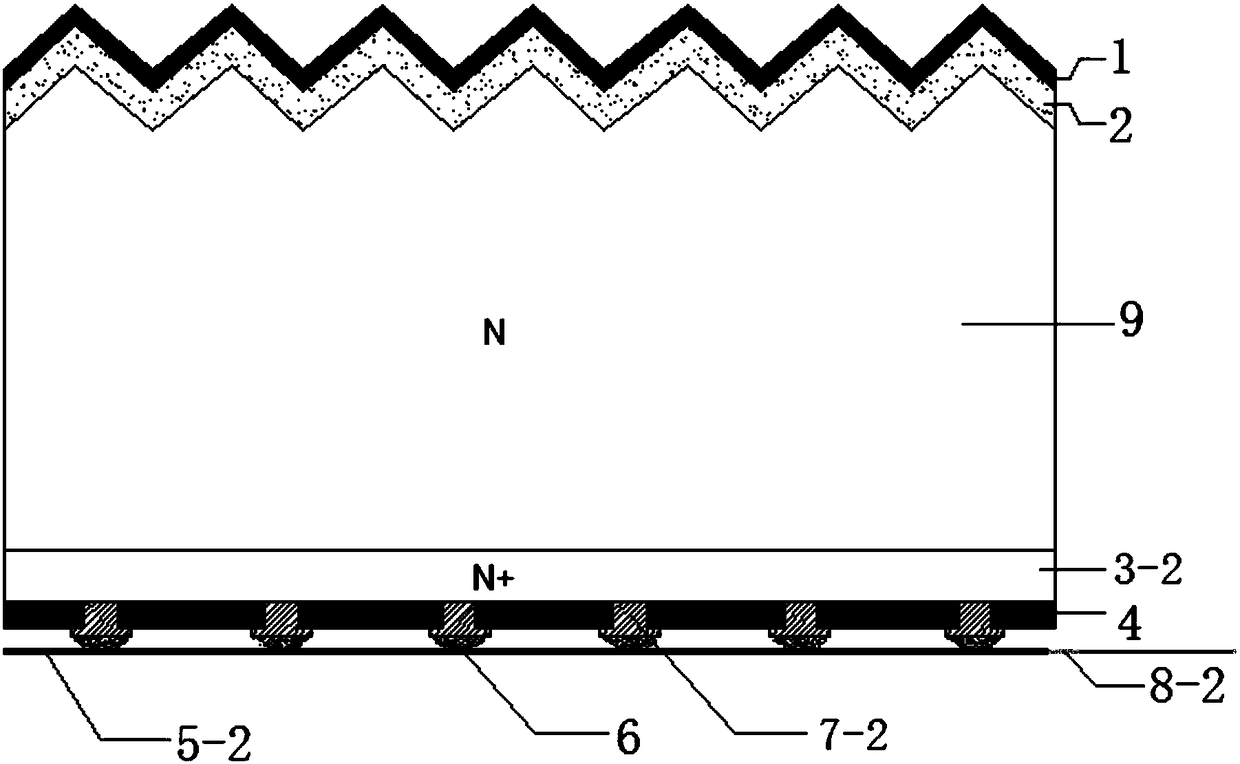
[0067] (2) On the back of the silicon wafer, ion implantation is used to form finger-shaped alternately distributed P-type doped layers and N-type doped layers. The width of a single P-type doped strip region on the back is 1mm, and the square resistance is 50Ω / □ ; The width of a single N-type doped strip region on the back is 0.5mm, and the square resistance is 50Ω / □. An 80Ω / □ N+ doped layer is prepared on the front side of the silicon wafer by ion implantation.

[0068] (3) Perform annealing treatment on the silicon wafer after ion implantation.

[0069] (4) Carry out chemical cleaning to silicon chip.

[0070] (5) Deposit 90 nm of silicon oxide on the front side of the silicon wafer, and deposit 30 nm of silicon oxide on the back side.

[0071] (6) The method of steel plate printing is used to make an array of local...

Embodiment 3

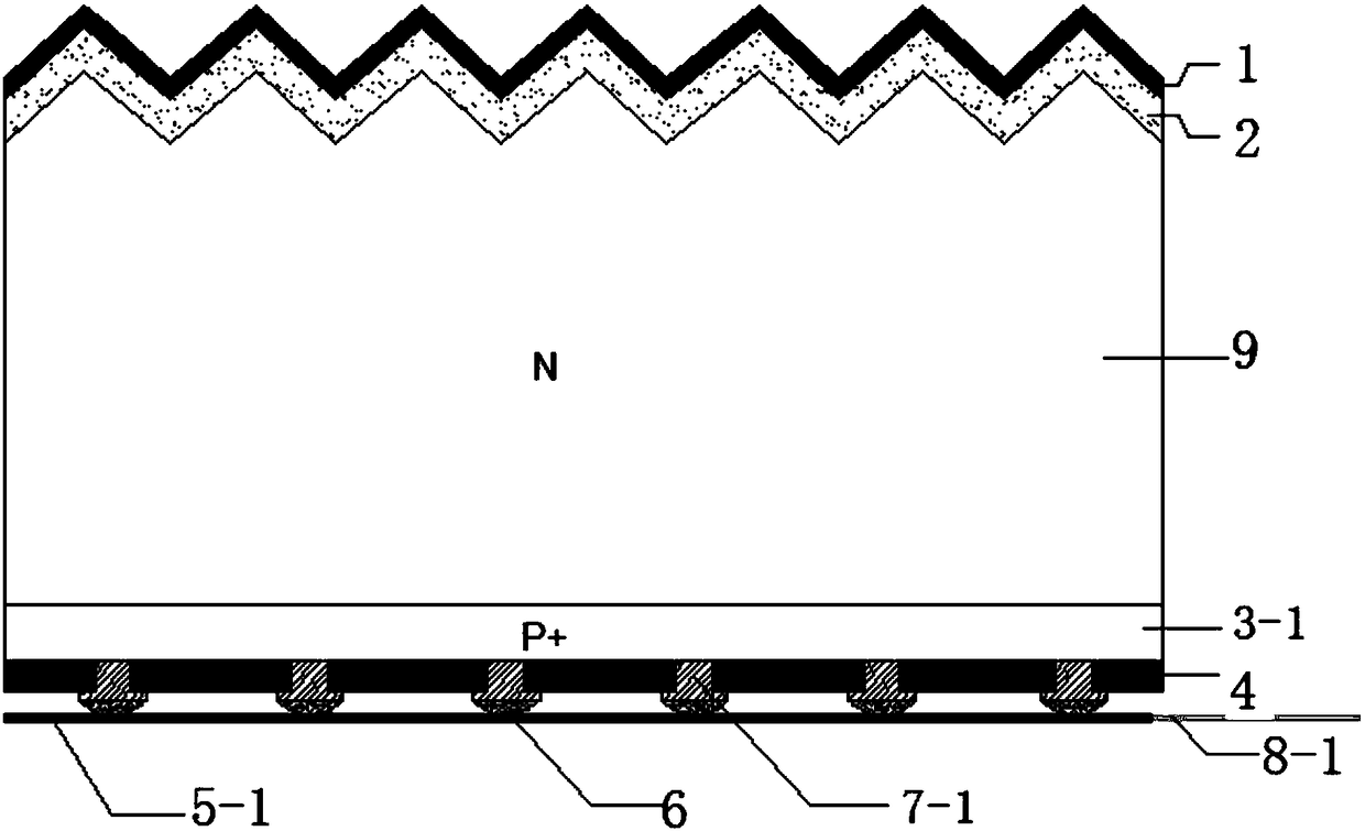
[0078] (1) The N-type monocrystalline silicon wafer is anisotropically etched in a KOH solution at about 80°C to obtain a pyramid structure on the surface.

[0079] (2) Print a boron-containing interdigitated diffusion mask layer on the back of the silicon wafer, and then perform thermal diffusion at about 750-950°C. The boron on the mask layer enters the silicon substrate after diffusion to form P-type doping layer, and the area where the mask layer is not printed, forms an N-type doped layer after phosphorus is diffused, and the P and N-doped layers are alternately arranged on the back of the silicon wafer. The width of the single P-doped strip region on the back is 2mm, and the square resistance is 60Ω / □; the width of the single N-doped strip region on the back is 1mm, and the square resistance is 60Ω / □. This process simultaneously forms a 90Ω / □ N+ doped layer on the front side of the silicon wafer.

[0080] (3) The phosphosilicate glass and borosilicate glass on the front a...


PUM


Abstract

The invention provides a full back electrode contact crystalline silicon solar cell structure and a preparation method thereof. The full back electrode contact crystalline silicon solar cell structure sequentially comprises an antireflection film / passivation film, a front N+ doping layer, an N-type silicon substrate, a back doping layer, a back passivation film and cell electrodes from top to bottom, wherein the back doping layer is formed by alternately arranging N-type doping regions and P-type doping regions at intervals; each cell electrode comprises local metal electrodes arranged in an array and fine metal guide wires; the local metal electrodes penetrate through the back passivation film; the local metal electrodes and the N-type doping regions and the P-type doping regions on the back surface form ohmic contact; the fine metal guide wires are combined with the local metal electrodes through a conductive bonding material to form local suspended fine grid line electrodes; and electrode leads are arranged at opposite ends of the P-type regions and the N-type regions on the back surface of a cell respectively and are used for exporting collected current. By the full back electrode contact crystalline silicon solar cell structure, the light shade area of grid lines is avoided, so that the conversion efficiency of the cell is improved; and meanwhile, the production cost is reduced by reducing the usage amount of metal paste.

Description

technical field [0001] The invention belongs to the technical field of solar cells, and in particular relates to a structure of a crystal silicon solar cell with full back electrode contact and a preparation method thereof. Background technique [0002] Since the first solar cell was born in Bell Laboratories in 1954, crystalline silicon solar cells have been widely used, the conversion efficiency has been continuously improved, and the production cost has continued to decline. At present, crystalline silicon solar cells account for more than 80% of the total global solar cell market, and the conversion efficiency of crystalline silicon cell production lines has exceeded 20%. The cost of electricity continues to shrink and is expected to be flat in the next few years. As a clean energy source, crystalline silicon solar cells play an increasingly important role in changing the energy structure and alleviating environmental pressure. [0003] If crystalline silicon solar cel...

Claims


Application Information

Patent Timeline
Patent Type & Authority Patents(China)
IPC IPC(8): H01L31/068H01L31/0224H01L31/18
CPCH01L31/022441H01L31/0682H01L31/1804Y02E10/547Y02P70/50
Inventor 李华钟宝申赵科雄
Owner LONGI SOLAR TECH (TAIZHOU) CO LTD
Why Eureka
Try Eureka